• Now offering merit based scholarship. Hurry up!
  • Bengaluru | Hyderabad
  • +91 - 97429 72744
Takshila VLSI
  • Takshila
    • About Us
    • Vision
    • Why Join Us
    • Blog
    • Apply as Trainer
  • Courses
    • For Freshers
      • Physical Design
      • ASIC Verification
      • Analog Layout Design
      • Design For Test
      • Analog Circuit Design
      • RTL Coding and FPGA Design
      • Embedded Systems Training
    • For Working Professionals
      • Physical Design-Part Time
      • ASIC Verification-Part Time
      • Analog Layout Design-Part Time
      • Design For Test-Part Time
      • RTL Coding and FPGA Design-Part Time
      • Analog Circuit Design
      • FINFET Layout Design Training
      • UVM Training
      • PERL Scripting
    • Online Courses
      • Physical Design Online
      • ASIC Verification Online
      • Analog Layout Design Online
      • Analog Circuit Design Online
      • Design For Test (DFT) Online
      • RTL Coding and FPGA Design Online
      • UVM Training Online
    • Online Course Videos
    • Free Demo Class
    • 1-Day Free VLSI Training
  • Course Calendar
  • Corporate
  • Placements
  • Contact
  • FAQs
  • Enquire Now.
  • Takshila
    • About Us
    • Vision
    • Why Join Us
    • Blog
    • Apply as Trainer
  • Courses
    • For Freshers
      • Physical Design
      • ASIC Verification
      • Analog Layout Design
      • Design For Test
      • Analog Circuit Design
      • RTL Coding and FPGA Design
      • Embedded Systems Training
    • For Working Professionals
      • Physical Design-Part Time
      • ASIC Verification-Part Time
      • Analog Layout Design-Part Time
      • Design For Test-Part Time
      • RTL Coding and FPGA Design-Part Time
      • Analog Circuit Design
      • FINFET Layout Design Training
      • UVM Training
      • PERL Scripting
    • Online Courses
      • Physical Design Online
      • ASIC Verification Online
      • Analog Layout Design Online
      • Analog Circuit Design Online
      • Design For Test (DFT) Online
      • RTL Coding and FPGA Design Online
      • UVM Training Online
    • Online Course Videos
    • Free Demo Class
    • 1-Day Free VLSI Training
  • Course Calendar
  • Corporate
  • Placements
  • Contact
  • FAQs

Analog Layout Design

Trainer
Mr.Ram
Category:
For Freshers/
₹90,000.00
analog circuit design training

Register Now
20 Students
Duration: 4 Months
Takshila VLSI Certificate

Custom Layout Design Courses & Analog Layout Design Training

COURSE DESCRIPTION

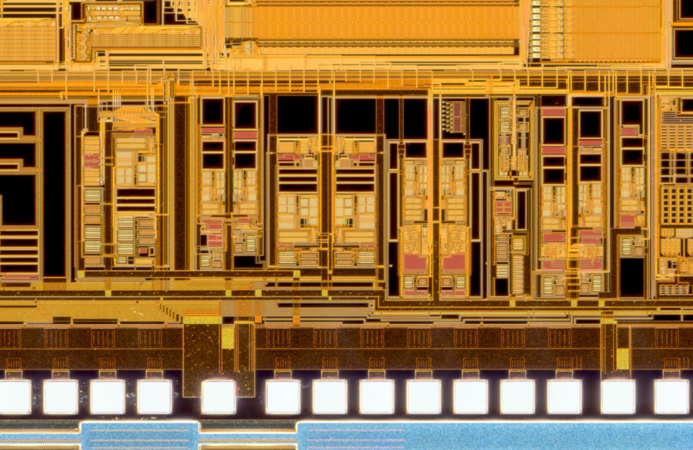
Analog Layout Design / Custom Layout Design / IC design training course mainly focused on giving hands-on practical exposure in doing chip layout design for a given analog & mixed signal design. By end of the course you will learn to work in Linux environment, schematic entry in EDA tool, placement planning, analog and digital layout design, routing and physical verification checks like DRC, LVS for typical analog circuits such as Opamp, PLL, Bandgap, LDO and standard cells. You will also understand fixing deep sub-micron process issues like Antenna, Latchup, EM&IR.

Course also focus on giving insights of the Analog circuit design and Simulation, IO Layout Training, Memory Layout Training as well. After completing the course, you will get opportunity to move into domains such as Analog & Mixed Signal Layout Design, Memory Layout Design, Standard Cell Layout Design, and I/O Layout Design.

Eligibility

  • B.E/B.Tech/Diploma in ECE/EEE.
  • M.E/M.Tech/M.S in VLSI System Design/Embedded Systems/Digital Electronics.

Features Highlight

  • Deep understating of MOSFET device physics and various key analog circuit designs.
  • Practical understanding of matching, shielding techniques.
  • Hands on exposure in fixing layout violations such as DRC, LVS, Antenna, Latchup, EM&IR.
  • Hands on experience in standard cell layout design, I/O Layout design, Memory Layout Design.
  • Critical Industry standard project execution under the guidance of 12+ year’s industry expert.
  • 24×7 Lab Support with classroom practice handouts and course material.
  • Soft skills development, job oriented analog layout design training with 100% placement assistance.

IC Design Training / Chip Layout training / Custom Layout Training

COURSE CURRICULUM

Module 1: Basics of Unix/Linux

Introduction and Working knowledge of UNIX/LINUX commands  
File handling skills in UNIX/LINUX  
Introduction to programming languages used in IC-Design  

Module 2: Introduction to Electronics and Circuits

Revision of Analog, Digital electronics, RLC Circuits  
Introduction to MOSFET Theory & CMOS Circuits  

Module 3: Design for Manufacturability Checks

Latch-up, Antenna Effect  
Electro-migration (EM), IR Drop & Self-Heat (SH)  
Electrical rule check (ERC) and Design rule check (DRC)  

Module 4: Deep sub-micron process challenges

Well proximity Effect (WPE), Length of Diffusion (LOD)  
Shallow trench Isolation (STI)  
Metal Density effects  

Module 5: Introduction to IC Circuit Layout

CMOS Fabrication Technology  
Introduction to Second order effects in MOSFET  
CMOS Stick Diagrams  
Introduction to IC Circuit Layout and Physical Verification tools  
DRC, LVS, ERC and Antenna checks  

Module 6: Analog Circuit Simulations

Introduction to Analog Design Environment  
Design of Inverter circuit  
Design and Parasitic Extractions of Inverter Layout  
Analysis of the INV Characteristics  
Understanding of the time delay concepts  

Module 7: Analog Circuit Layout Design Techniques

Common centroid & Interdigitation matching techniques  
Critical signals shielding techniques  
Constraint & Module based floor planning techniques  
Guard / Seal ring techniques  

Module 8: Custom Layout Techniques

STD Cell Layout design techniques  
I/O Layout design techniques  
Memory Layout Design techniques  

Module 9: Basic Analog Circuit Layout Design

Layout Design & Physical Verification of Operation amplifier  
Layout Design & Physical Verification of Voltage Controlled Oscillator  
Layout Design & Physical Verification of Band gap Circuit  
Layout Design & Physical Verification of Current mirror  

Module 10: Layout Design of Critical Analog Circuits

Advanced/Critical Analog Circuits  
Complete Physical Verification Checks required for a Successful tape-out  

Module 11: Industry standard Project Execution

Working on Critical Analog Circuits that are important in Industry  

Module 12: Mock Interviews & Personality improvement

Analog Layout Design Demo Videos

4 Reasons That Make Our Analog Design Course the Greatest Of Them All

Yes! We are proud to say that our analog layout design training is the greatest of them all. Generally, analog design means circuit design. It involves converting specifications into transistor-level circuits, simulating, as well as verifying the design’s functionality and ensuring that it works on silicon.

But circuit diagrams on paper or PCs can’t be manufactured thus comes the implementation part. Analog layout designers, who have undergone chip layout training, transform the circuit diagrams into polygons which are then utilized as masks for lithography steps to implementing the circuits on silicon. With the present level of technological advancement, it now demands lots more capabilities. It is these capabilities that we infuse into our students via our foremost analog layout design course. Some of the foremost reasons why our course is the greatest of them all include;

1. The Foremost Analog Layout Training Institutes

We have some of the foremost analog layout training institutes you will ever find, around the whole world. We have spread our network for service provision quite wide. This is as we run the foremost analog layout training institutes in Bangalore as well as the foremost analog layout training institutes in Hyderabad. The main focus of our institutes is to make every single budding engineer understand the physical design of ICs from circuit to layout to tapeout, developing the right physical layout representation for every single analog function with in-blocks to enable the IC fabrication process.

While studying this course with us, for each student, a lot more emphasis is placed on providing quality learning via lab practical that is backed by theoretical concepts that are taught by the foremost experts of the industry during classes as well as in laboratory sessions.

2. What You Will Learn

Our analog layout training focuses mainly on providing hands-on practical exposure to executing a chip layout design for any given analog and mixed signal design. By the time you complete the course, you will understand how to work in Linux environments, placement planning, routing and physical verification checks such as DRC, LVS for usual analog circuits like PLL, LDO, Opamp, Bandgap, and standards cells, schematic entry into EDA tools, as well as analog and digital layouts design. Also, you will understand how to fix deep issues of sub-micron processes such as Latchup, Antenna, as well as EM&IR.

Also, our course focuses on providing insights into analog circuit design and simulation, memory layout training, and IO layout training. After you have completed your course, you are allowed to enter into other varying domains like standard cell layout design, analog, and mixed signal layout design, as well as IO layout design.

3. Analog Layout Training with Placement

One of our most unique features is that we offer layout design training with placement in some of the foremost firms in the whole world. Whether you choose to go for our custom layout training, IC design training, IO layout training, layout design training, memory layout training, or any of our other numerous analog and mixed signal layout courses, by the time you complete your studies, we provide you with 100% placement support. Our major aim is to help all engineers who graduate with us to build the most successful career they can in the VLSI industry.

4.Our Affordable Costs

We offer the best low-cost analog layout training you will ever get throughout the entire industry. If you compare the cost of our courses to the quality of teachers, materials, as well as lab resources that we offer, then you will understand that our students get way more value than what they have paid. The analog design training that is offered by our layout training institutes in Bangalore is among the foremost training you will ever get, yet it’s offered at one of the lowest prices you can equally get in the entire industry. In fact, we even bundle our amazing finfet layout training into the course for our students. These are among the foremost reasons why the majority of VLSI students prefer to study with us.

Layout engineers are the ones who are responsible for the development of layouts from scratch. So, they need to be properly trained. For this reason, we offer one of the greatest analog layout design courses you can ever get in the whole world. Our training are delivered using the most trending and unique methodologies and technologies. We ensure that our students eventually become real experts at what they do.

Frequently Asked Questions

1. What is the duration of the Analog Layout Design course?

The course is 4 months long. Throughout the Analog Layout Design course, you will be given detailed instruction and practical exposure, along with many chances to enhance your skills in analog layout design.

2. What kind of certification will you receive after the course?

After the course, you will receive a Takshila VLSI Certificate, acknowledging your proficiency in analog layout design education. Getting this certification can enhance your credentials and increase your competitiveness in the employment industry.

3. Can I take this course if I am working?

Yes, This course is created to be flexible, providing weekend classes and lab access 24 hours a day, 7 days a week. It enables you to disrupt your present job while also advancing in learning analog layout design.

4. How does this course prepare me for a career in Analog IC layout design?

Our course prepares you by offering practical, real-world projects and extensive training in analog IC layout design. You’ll work with industry-standard tools and receive dedicated job placement assistance to help you secure a position in the field.

5. What will your Analog Layout Design course teach?

Our Analog Layout Design course will cover the fundamentals of VLSI analog layout design. It involves actual practice in schematic entry, placement planning, routing, and physical verification checks. The class includes basic and advanced subjects to prepare you for developing and testing analog ICs effectively.

6. What is the fee structure of this course?

The price of the Analog layout design for the VLSI course is established at a competitive rate to provide excellent value. For additional details on fees and payment methods, contact us directly or visit our admissions webpage on the site. We offer various payment choices and financial assistance to help lower the cost of the course for everyone.

About Instructors

Mr.Ram
A VLSI Professional with 15+ years of rich experience in Analog Mixed-signal Layout design. Worked with Tier 1 Semiconductor Product and Service companies and also Product based startup companies which helped me to understand the learning curves and business models. Having facilitative leadership skills and having a proven track record with leading teams on-site & offshore design centers.

Register Now
20 Students
Duration: 4 Months
Takshila VLSI Certificate

Course categories

  • For Freshers (7)
  • For Working Professionals (9)
  • Online Courses (7)

Working hours

Monday 9:30 am - 6.30 pm
Tuesday 9:30 am - 6.30 pm
Wednesday 9:30 am - 6.30 pm
Thursday 9:30 am - 6.30 pm
Friday 9:30 am - 6.30 pm
Saturday 8:00 am - 6.30 pm
Sunday 8:00 am - 6.30 pm

Social Network

Takshila VLSI institute is among the top 10 VLSI training institutes in India. At Takshila, we understand the changing demands in the field of VLSI.
Our courses are designed to offer students hands-on experience in industry trends.

Quick links

  • Apply as Trainer
  • Course Calendar
  • Placements
  • Why Takshila VLSI
  • Free Demo
  • FAQs

Useful links

  • Privacy Policy
  • Refund Policy
  • Terms and Conditions

Contact Us

  • Marathahalli, Bengaluru - 560048
  • Madhapur, Hyderabad - 500081
  • +91-9742972744
  • info@takshila-vlsi.com

Social Network

Copyright © 2024. Takshila-VLSI. All Rights Reserved.
  • Home
  • About Us
  • courses
  • Contact Us
Search