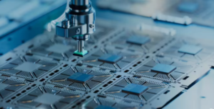
As semiconductor technology transitions to smaller geometries, physical design is no longer simply a matter of placing cells and routing wires. The engineers are now confronted with a different degree of complexity; it is less about margins and more about variability, and each design decision is significant. When using or writing about Advanced node VLSI, it is essential to understand the modern physical design challenges. This blog explains how advanced nodes differ, why those differences exist, and how engineers adapt their work to build chips on next-generation VLSI nodes.
Why Physical Design Becomes Harder in Advanced Nodes
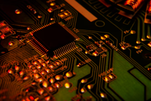
Shrinking geometries bring significant physical design challenges related to variability, power density, and manufacturability. In Advanced node VLSI, traditional assumptions about routing resources and timing no longer hold. Designers must confront tighter design rules, multi-patterning constraints, and increased sensitivity to process variations.
These challenges in advanced-node VLSI design directly affect yield and performance. As a result, SoC physical design techniques must evolve to address complexity at the block and full-chip levels, especially for next-generation VLSI nodes.
Congestion, Routing, and Layout Optimization
Routing congestion is one of the most obvious Physical design challenges for advanced nodes. Dense standard cells, limited routing tracks, and complex IP integration increase the difficulty of clean routing. Effective VLSI layout optimization is essential for balanced performance, area, and power.
Engineers rely on advanced node-routing strategies, including early congestion analysis, layer-aware routing, and strategic block placement. These methods improve routability in advanced node VLSI designs and ensure predictable results across large SoCs.
Timing Closure and Power Integrity Issues
Timing closure in Next-generation VLSI nodes is much more difficult due to increased resistance, capacitance, and variability. Clock skew, crosstalk, and IR drop are common advanced node VLSI design challenges that can derail schedules if not addressed early.
Current [SoC] physical design methods integrate power planning, clock-tree optimisation, and incremental timing analysis from the outset. Proper VLSI layout optimization can reduce timing issues without compromising signal integrity or requiring reworking.
Role of Physical Design Automation at Advanced Nodes
Given the size and complexity of today’s chips, physical design automation has become a necessity. Automation streamlines repetitive tasks, enables analysis of large datasets, and accelerates design convergence.
In advanced node SoC design, automated processes help arrange components, resolve routing issues, and perform final checks. Well-tuned Physical design automation improves productivity while reducing human error, an important factor when dealing with tight constraints in advanced node VLSI projects.

Preparing for Next-Generation VLSI Nodes
The mindset for designing next-generation VLSI nodes has changed. Engineers need to combine strong knowledge with hands-on experience in advanced routing methods, power integrity checks, and scalable physical design techniques for System-on-Chip (SoC) design.
Successful teams plan for physical design challenges, rely on established VLSI layout optimisation methods, and continually deal with new tools and rules. This strategy is an offensive approach to delivering quality silicon on demand.
Conclusion: Building Expertise to Overcome Physical Design Challenges.
Learning physical design challenges at advanced nodes combines theory, tools, and real-world problem-solving. Congestion, timing, automation, and scalability of advanced node routing strategies in VLSI are more critical than ever.
Engineers can develop hands-on skills in advanced node SoCs and physical design automation by participating in training and exposure programs offered by organizations such as Takshila VLSI. By deepening your knowledge of SoC physical design techniques and preparing for next-generation VLSI nodes, you will be well-positioned to address current physical design challenges and become a qualified VLSI expert.