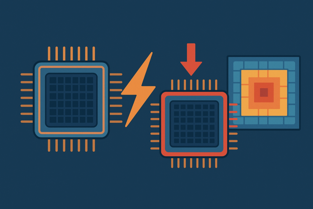
One of the most neglected, but most important aspects in modern chip development is power delivery. Engineers tend to consider timing, routing, and placement, yet without robust power integrity, even the most efficient design might not work in silicon. With the reduction in the size of technology nodes and growth in switching activity, it has become more complicated than ever to manage power. This is where it is necessary to know Power planning in chip design, know IR drop in VLSI, and carry out IR drop analysis properly. In this guide, divide the basics into a simple, easy-to-understand manner and demonstrate how efficient VLSI physical design power planning guarantees the longevity of chips.
Why Power Planning Matters in Chip Design
Any integrated circuit is supported by a strong power delivery network. Efficient power planning in chip design guarantees that voltage does not change around and that all the functional blocks do not malfunction as a result. Due to the increase in clock speed and the reduced size of transistors, power density is increasing, and it is more difficult to ensure voltage stability. That is why designers need to depend on the structured VLSI physical design power planning to minimize the resistance in metal layers, optimize power straps and minimize voltage droop. As a correct implementation, it enhances performance, minimizes noise, and eliminates long-term degradation due to Electromigration in VLSI.
The grid plan is not only necessary but must be well-planned to ensure the performance and also ensure the integrity of silicon over the lifecycle of the chips.
Understanding IR Drop in VLSI Systems
The voltage drop that results when a current is passed through the resistive metal layers of the power grid is called IR drop in VLSI. A minor decrease may lead to timing failures, reduced switching, or total functional errors. A small IR drop can be an important concern, especially with new technologies where transistor threshold margins are reduced by a factor of four. This is the reason why contemporary designers employ structured IR drop analysis to test the changes in voltages over the chip.
IR drop is one of the most critical issues during VLSI physical design power planning because it has a direct influence on performance, stability, and reliability.
Types of IR Drop: Static vs Dynamic
Static IR Drop
Static IR drop occurs when the chip is operating at a constant or low switching activity. This form of voltage drop is caused mainly by steady-state current flow across resistive power lines. It helps designers estimate worst-case voltage levels under non-switching conditions and is a critical part of early IR drop analysis.

Dynamic IR Drop
Dynamic IR drop is more complex and occurs when multiple cells switch simultaneously, causing sudden spikes in current demand. This leads to rapid voltage dips, which can significantly affect high-speed logic and memory. When developing strong power planning in chip design, engineers must account for these transient dips to avoid performance collapse in real applications.
Both forms of IR drop must be managed efficiently to ensure a smooth and predictable VLSI physical design power planning process.
Key Factors Contributing to IR Drop
- Increased switching activity
- Narrow metal layers at advanced nodes
- Long-distance current paths
- High power density blocks
- Poor placement of Decoupling capacitors in VLSI
- Excessive resistance in the power grid
These factors collectively add complexity to the IR drop in VLSI and often require iterative refinement of the power grid.
How IR Drop Impacts Chip Performance
Uncontrolled IR drop may slow down circuits, change timing closure objectives and produce unreliable failures. Dynamic droop has a serious effect on clock distribution and signal propagation. The exposure speeds up Electromigration in VLSI, which reduces metal reliability. That is why designers do elaborate IR drop analysis at various points of development.
Inadequate optimization of VLSI physical design power planning may cause silicon failure, expensive re-spins and life cycle degradation of the product.
Best Practices to Reduce IR Drop
- Use wider power rails and dense grid structures
- Place decoupling capacitors in VLSI close to high-switching blocks
- Optimize macro placement to shorten current paths
- Strengthen wise between metal layers
- Analyse both static IR drop and Dynamic IR drop thoroughly
- Improve distribution through multi-layer grids
These methods collectively strengthen power planning in chip design and help engineers build high-performance, low-risk architectures.
Conclusion
Constant power delivery is a must in the current sophisticated semiconductor world. The study of IR drop in VLSI, the recognition of voltage droop causes, and the practices of strong IR drop analysis can guarantee reliability between the tape-out and deployment. Successful VLSI physical design power planning is riskless, performance-enhanced and maintains high functionality of advanced chips under real work load conditions.
Takshila VLSI offers industry-specific training that encompasses all aspects of power planning in chip design to advanced sign-off methodology, such that learners can accumulate skills to have a successful career in the semiconductor industry.


