Due to constant improvements in technology, the field of VLSI remains one of the most vibrant and influential domains. It is a part of modern electronics-from a smartphone to an advanced computing system. What would a typical day for a VLSI student be? How does the complexity of circuit design, digital systems, and industrial demands shape this? Let’s take a tour of what a day in the life of a VLSI student is and see the skills, challenges, and opportunities that could be shaping their experience.
Early Morning – Start of a New Day
A typical day for a VLSI student starts with eagerly looking forward at dawn towards the battles and learning ahead of them. The morning is usually spent revising the notes that were taken from yesterday’s lectures or getting ready for today’s lectures. Students studying VLSI realise they would apply all this knowledge now used in learning to their real working life tomorrow; thus, they must gain complete mastery of all.
Most of the VLSI topics are reviewed within the early hours. Some of these regular topics of subjects one encounters in a VLSI curriculum include the design of logic transistor-level design semiconductor physics, as well as digital signal processing. These issues are challenging and require much attention. Most VLSI students’ days begin with browsing through slides of lectures, text or internet-based resources on those topics.
Attendance of Classes – A Detour Through VLSI Concepts
After all the morning preparation is done, they head off to attend classes. The typical routine is like this: a lecture class where lectures are kept in mind while instructing the deeper theoretical and practical aspects of VLSI technology. This includes the basic concepts behind integrated circuits and chip designs, as well as the latest emerging technologies in the semiconductor field.
The lectures cover many and varied topics, such as CMOS technology, logic gates, digital design, and others that are quite challenging but more advanced than FPGA (Field-Programmable Gate Arrays) and ASIC (Application-Specific Integrated Circuit) design. These topics are the basics of VLSI student life and are essential for a career in VLSI.
Hence, what a VLSI student learns as an informal requirement of his curriculum is essentially offered through practical application. The students are taught computer-aided design tools and techniques used by professionals in the VLSI industry, such as design automation tools, simulation software, and circuit analysis tools, including Cadence and Synopsys.
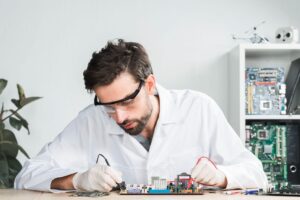
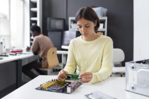
Lab Sessions-Practical Learning
Lab sessions are a key part of VLSI student life. They transform the theory of class into practice. Students spend a good number of their working hours in labs conducting simulations, circuit designs, and other designs. Laboratory sessions also expose them to the industry-grade software used in actual VLSI designs.
In lab work, students are exposed to designing and testing digital circuits or even simulating the functioning of various semiconductor devices. They can design logic gates, multiplexers, and any very complex circuits. Once more, only hands-on work hones one’s problem-solving ability. Precision and care start to emerge here. Minute mistakes in laboratory designs cause important problems later. For that reason, precision and meticulousness are required of the students in VLSI.
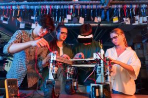
Group Discussions and Collaborative Learning
Success in VLSI requires teamwork. So, most of a VLSI student’s day is spent working together to solve a very complex design problem. It could be assigned as a team project for a class assignment, or it could be teamwork to simulate a difficult circuit. Success in VLSI requires teamwork on a regular basis. VLSI students often get together to discuss the most challenging design problems and come up with solutions.
These group discussions are part of the VLSI training. They nourish creative thinking, problem-solving, and knowledge sharing. VLSI students are exposed to various views, which may help them solve problems from different angles. This is similar to working in the VLSI industry, where multiple ideas come together to form complex designs.
Afternoon – Focused Study and Personal Projects
Following group activities and lab sessions, the afternoons are usually occupied with assignments, personal projects, and examination preparations for LSI students. Student life at VLSI is challenging and demanding; efficient time management is always necessary for coursework, project deadlines, and self-study sessions.
This can all be done within afternoons reserved for such complex topics as circuit optimisation, power consumption analysis, or even timing analysis as students dig into them. Of course, not all personal projects are in his interest and might range from some custom VLSI chip or the latest semiconductor trend going into machine learning and AI acceleration of hardware.
It is also a period during which students can obtain internships or part-time jobs in VLSI companies. Internships are a dominant component of every student’s experience. They provide them with real-life exposure and eventually enable them to apply theoretical know-how to practical and real-life settings. An internship provides a good foundation for an excellent career in the VLSI industry and gives students a real taste of life and working in the industry.
Networking and career development in the evenings
Generally, most VLSI students will spend their afternoons networking and deliberating on what to expect from the workplace because job opportunities regarding VLSI in the market are limited. In other words, the university’s hosting of a large number of workshops and seminar sessions, as well as any networking, encourages invited lecturers on VLSI technology development to seek an opinion from the industry.
Most evenings are spent in guest lectures, webinars, and virtual workshops to keep the students updated with the latest trends in VLSI design. Besides, it is more important to get an overview of how to choose within the VLSI domain at the chip-design level, verification/validation, or testing.
Above those are some of the few VLSI students. They do a bit of prep work on life itself, and towards the end of all that, they participate in career fairs and look one last time over resumes or portfolios they have developed with all their VLSI coursework. By then, during the evening hours, the VLSI learner is positioned well for action designed toward launch time.
Work-life and Self-Care
Life as a VLSI student can sometimes be very tiring, with long hours spent in class, laboratories, and cramming for exams. However, ensuring a healthy balance between work and life is essential for long-term sustainability. Self-care is as important as academics, and students in the VLSI stream are constantly reminded of this.
Indeed, most of the students want to spend their free time relaxing, doing hobbies, or keeping ties with friends and family members after a day full of studying and problem-solving. Downtime is required because these refresh and equip them for the next day’s tasks. A healthy balance in the life of VLSI students maintains motivation, renewal of energy, and focus on the goal.
Conclusion – Bright Future
A day in the life of a VLSI student is filled with learning, problem-solving, collaboration, and planning for the future. The skills gained through this rigorous training, coupled with hands-on experience, prepare students for an exciting life in VLSI industry. From chip design to semiconductor technology, the opportunities are vast for those who are passionate about innovation and technology.
Students venturing into the creation of a very successful career first take steps within platforms like Takshila for their growth towards success. They provide extensive and comprehensive VLSI training. The courses equip the participants with the latest understanding that would make their practical experience well integrated with the existing industry practices as well. Takshila makes sure that VLSI students are well-equipped for their careers by providing expert-led courses, hands-on projects, and real-world industry exposure in the domain of semiconductor technology.