


Engineers frequently wonder about the comparison of ASICs and FPGAs in the contemporary fast world of semiconductor design. Both technologies have their advantages, applications, and methodologies in verification. So, understanding

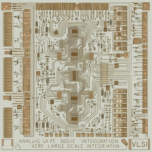
An analog layout design certainly defines the area where the conceptual brilliance of circuits turns into a physical reality, ensuring performance, precision, and dependability. As an amateur, one may find

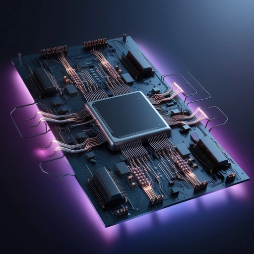
A Physical Design engineer in the semiconductor industry performs the critical task of taking abstract specifications for chips into tangible, working hardware. As demands for smaller, faster, and more efficient
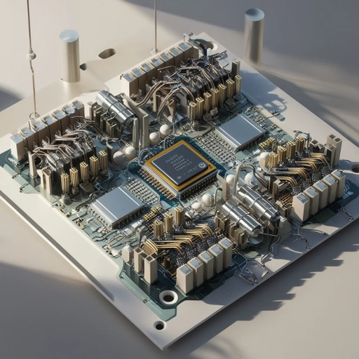
The semiconductor fabrication process is the heart of the technological revolution, hence allowing for advanced development of electronic devices. Today, though, with growing demand for faster and smaller chips to
Low power design in VLSI has emerged one of the critical requirements in modern semiconductor design. The requirement of compact devices that can have an extended period of battery life
In VLSI designs, the term symmetry in analog layout does not have any aesthetic value it will bring but is a decisive factor affecting the functionality and reliability of the

Analog layout design in RF circuits may be only done with much precision and with firm know-how of analog and RF principles. They present a very important link in any

Power and integrity have emerged as crucial elements to ensure that electronic systems function and behave properly, especially in the domain of VLSI design. With the exponential increase in the

Verification is the critical step in the ASIC designing process concerning ensuring whether the final product works just as expected. The preferred language for ASIC verification turned out to be

Achieving timing closure in VLSI physical design from graph partitioning to timing closure is crucial for chip performance and reliability. This might sound like rocket science to a newcomer, but