


The need for advanced learning and specialized training in VLSI technology has never been as high as it is now. The semiconductor and electronics industry is expanding at an unprecedented

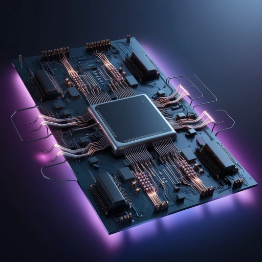
VLSI is the heart of modern electronics, powering microprocessors, memory chips, and integrated circuits for countless devices. Be it a beginner who is eager to break into this dynamic industry

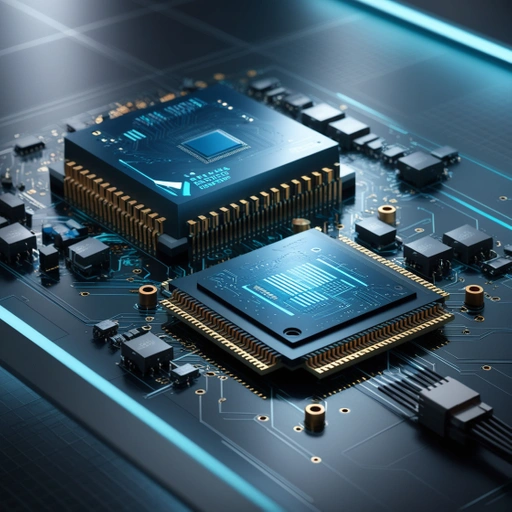
Fast advancements in technology have revolutionized the electronics industry, with VLSI (Very Large Scale Integration) design emerging as a highly sought-after skill. This expertise unlocks tremendous career opportunities, making it

The verification phase is as important as the design in ASIC (Application-Specific Integrated Circuit). It gives assurance that the final product will function flawlessly and meet all specifications required. In
Engineers frequently wonder about the comparison of ASICs and FPGAs in the contemporary fast world of semiconductor design. Both technologies have their advantages, applications, and methodologies in verification. So, understanding

An analog layout design certainly defines the area where the conceptual brilliance of circuits turns into a physical reality, ensuring performance, precision, and dependability. As an amateur, one may find

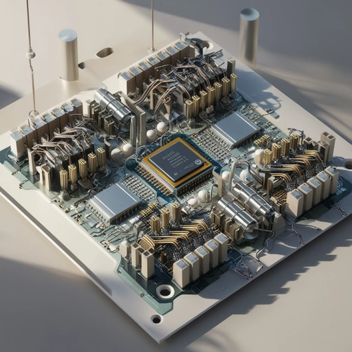
A Physical Design engineer in the semiconductor industry performs the critical task of taking abstract specifications for chips into tangible, working hardware. As demands for smaller, faster, and more efficient
The semiconductor fabrication process is the heart of the technological revolution, hence allowing for advanced development of electronic devices. Today, though, with growing demand for faster and smaller chips to
Low power design in VLSI has emerged one of the critical requirements in modern semiconductor design. The requirement of compact devices that can have an extended period of battery life
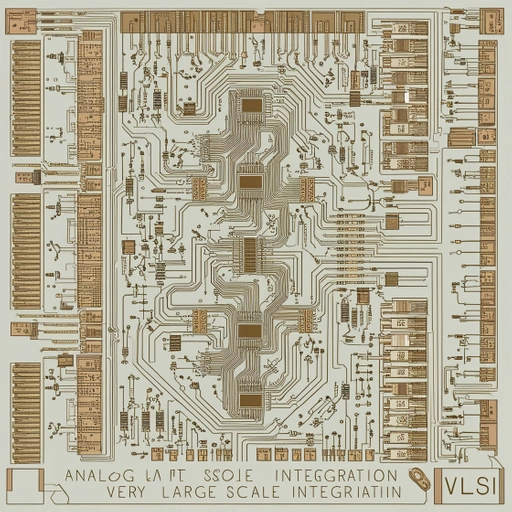
In VLSI designs, the term symmetry in analog layout does not have any aesthetic value it will bring but is a decisive factor affecting the functionality and reliability of the