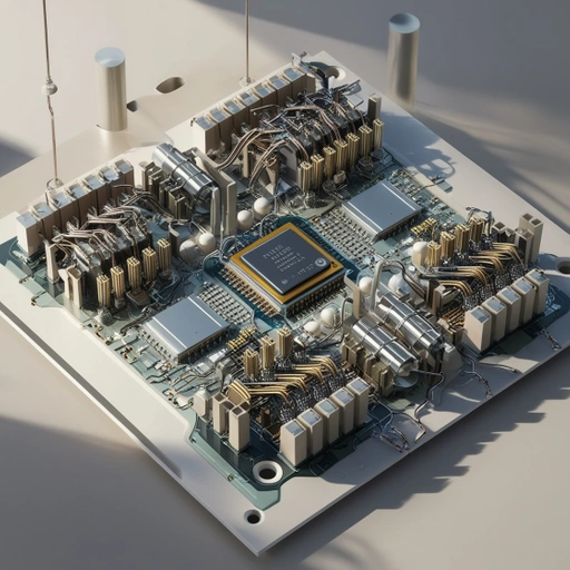
Low power design in VLSI has emerged one of the critical requirements in modern semiconductor design. The requirement of compact devices that can have an extended period of battery life and energy consumption resulted in engineers making innovative low power design techniques possible in VLSI. Since physical design is important while power efficiency is critical and performance and reliability of ICs are maintained, the importance lies there. This blog discusses the techniques and best practices involved in low-power VLSI design techniques to optimize energy consumption during the physical design process.
Low Power Design in VLSI
Integration of smartphones, wearables, and IoT sensors in daily life recently has led to the focus on power efficiency issues. Power reduction increases battery life and decreases heat dissipation. It also lowers data center operational costs. Design techniques involving low power design in VLSI have these objectives but also face issues like performance trade-offs and circuit complexity.
Important Power Components in VLSI Design
Before discussing techniques, one must first understand that the major consumers of power in VLSI circuits are:
- Dynamic Power: The switching activities present in the circuit result in dynamic power. It is a function of the switching frequency, voltage, and capacitance.
- Static Power: In this type of power, one finds leakage currents in the transistors when these are not switching.
- Short-Circuit Power: This arises from the direct current paths when there is a transition of the logic states.
Physical design engineers maximize these components while relying on various power optimization techniques in VLSI at the design stage.
Low Power Physical Design Techniques
1. Clock Gating
Clock Gating is one of the most popularly used low power VLSI design techniques. It allows dynamic power consumption reduction by disabling the clock signal to inactive circuit blocks. This ensures that unnecessary switching activity takes place, thus saving a significant amount of power.
2. Multi-VDD Design
Other parts of the die can operate at varying supply voltages as this enables important blocks to maintain high voltages for best performance while less-senior blocks perform at lower voltages for maximum efficiency. This hierarchical approach balances performance with power.
3. Power Gating

Sleep transistors are used to switch off the power supply to idle blocks, effectively reducing static power consumption. This approach significantly lowers leakage current during idle periods, enhancing overall power efficiency.
4. Dynamic Voltage and Frequency Scaling (DVFS)
DVFS is an advanced technique wherein the processor voltage and frequency are varied dynamically as per the workload requirement. In this approach, energy usage gets optimized without losing performance when the activity reaches its peak.
5. Placement and Routing Optimization
In physical design, cells are placed and routed efficiently, so the capacitance and resistance within interconnects are reduced to the minimum. Shorter interconnects imply less power dissipated and signal propagation faster.
6. Low Power Libraries
Application of low power optimized standard cell libraries in VLSI ensures all the design blocks by default are quite efficient. Such libraries do contain low leakage cells, which prove to be the most contributing factor for the reduction of static power.
7. Clock Tree Power Reduction
Clock Networks consumes a significant fraction of the dynamic power. Techniques such as clock tree synthesis with low power constraints, and reducing clock skew will be quite efficiency enhancing .
Best Practices for Low Power VLSI Design</h2>
Early Power Estimation
Power considerations should begin during the architectural design phase. Tools for early power estimation help designers predict and mitigate power issues before physical design begins.
Partitioning and Hierarchical Design
- Logical Partitioning: Logical partitioning basically ensures that the blocks are optimized for power.
- Hierarchical Approach: The design in VLSI with a hierarchical approach makes low power design technique simple and improves the overall efficiency.
Leakage Management
The leakage currents contribute enormously in terms of static power for nanoscale designs. Various techniques such as body biasing, transistor sizing and gate oxide optimization are used for leakage minimization.
Power Intent Specification
Deployment of formats such as Unified Power Format (UPF) and Common Power Format (CPF) ensures that the power-saving measures are well integrated across design tools and stages.
Simulations and Validation
Periodic simulations with power-aware tools ascertain that all the applied power optimization techniques are highly effective for VLSI. They indicate directions where additional improvements are possible.
Applications of Low Power VLSI Design
Low power design is heavily important in the following domains:
- Mobile and Portable Devices: Increase the battery life for smartphones, tablets, and wearables
- Internet of Things (IoT): Energy efficient sensors and connected devices.
- Automotive Electronics: Make High-Power Saving in ADAS
- Data Centers: Low energy cost, better thermal management for high-performance computing
Challenges in Low Power Design
The potential of low-power design techniques in VLSI is undeniable, but their implementation comes with several challenges, including:
- Performance Trade-offs: Salvaging power with computational performance
- Design Complexity: Power domains in Large designs
- Verification Overhead: High verification of low power intent along with functional correctness.
If the right strategies and tools are adopted, then all these challenges can be easily mitigated.
Conclusion
Symmetry is the heart and soul of excellence in VLSI analog design and helps to minimize mismatches, enhance noise immunity, and improve circuit performance and reliability. A well-done analog layout focuses on applying high techniques to achieve symmetry using common-centroid placement, dummy devices, and symmetric routing. Such techniques lead to robust designs that reflect a high degree of industry standard, enabling designers to handle even the most challenging tasks.
Takshila VLSI brings these concepts together to prepare students as champions of analog layout design. Industry-aligned curriculums from top mentors, with hands-on project experience, will keep you better geared for real-world challenges. Our services cater for fresher and professional alike, to be strong on symmetry in analog layouts, pushing the career boundaries to the best the VLSI has to offer.
Begin your journey with Takshila and make your dreams come true.


