




Ask any physical design engineer what kept them at their desk past midnight, and there’s a good chance the answer involves VLSI congestion. It’s one of those problems that sounds

Ask any hiring manager in the semiconductor industry what separates a job-ready VLSI candidate from one who needs months of retraining, and the answer almost always comes back to tools.
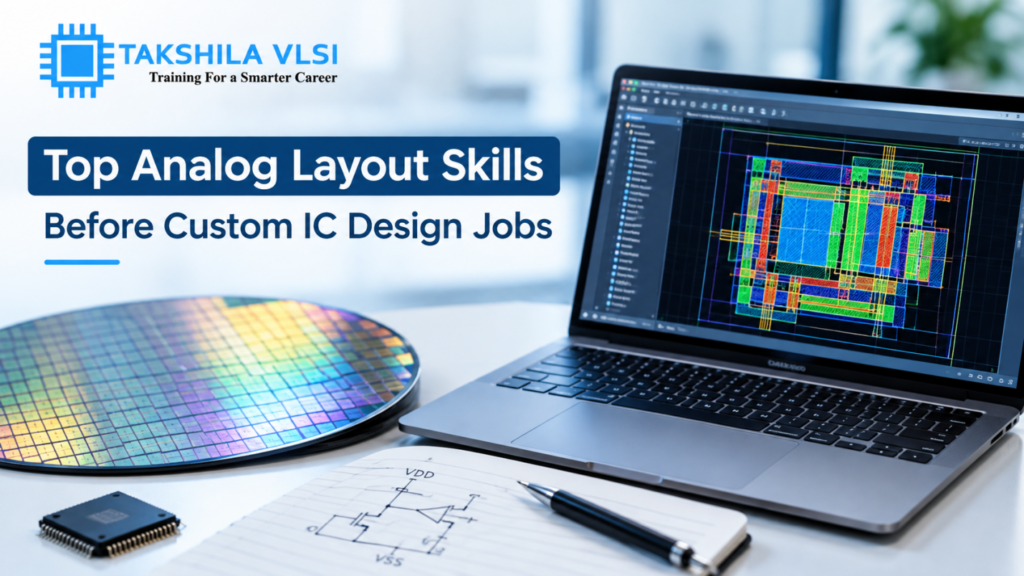
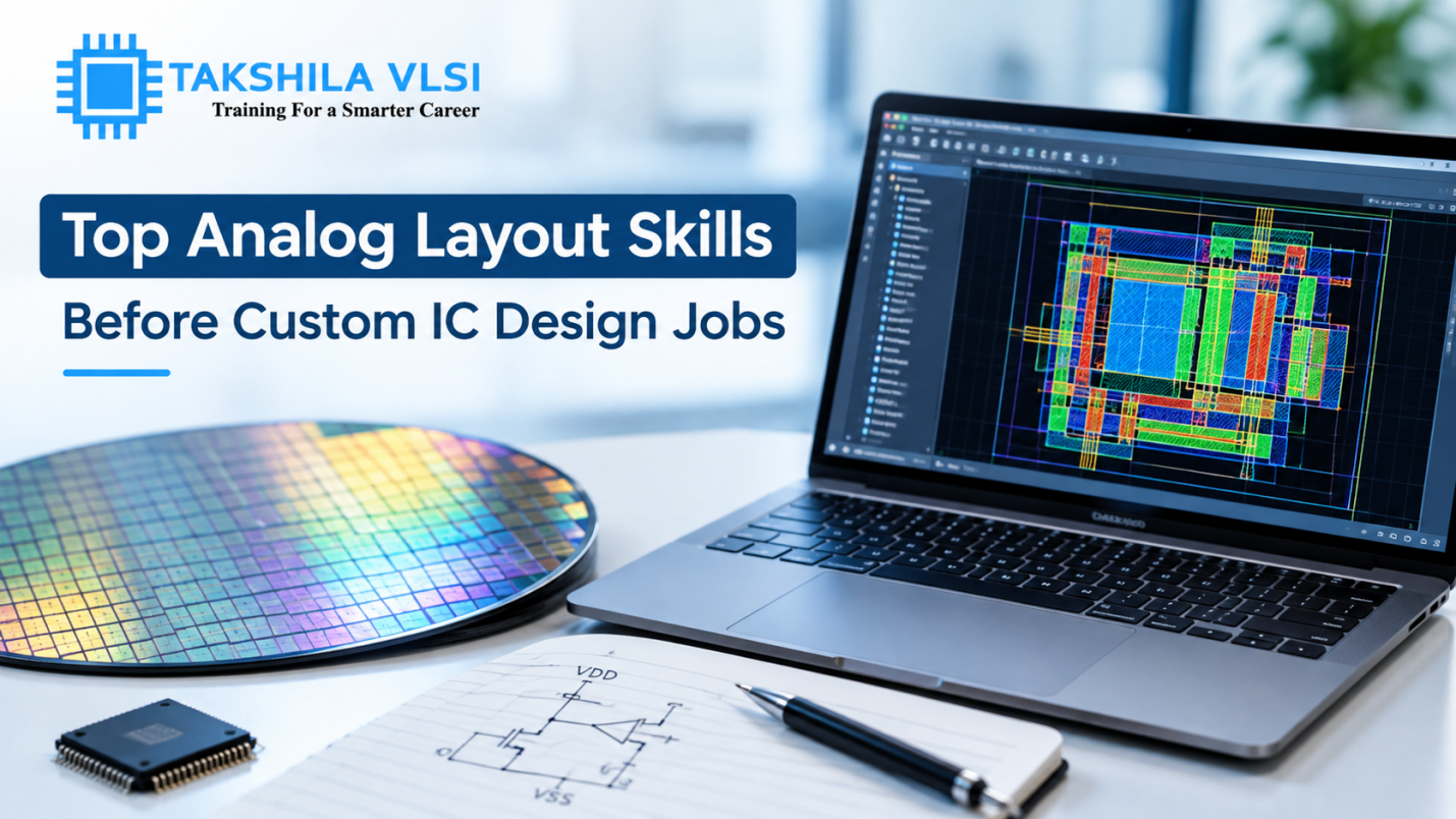
Analog layout design occupies a curious space in VLSI it is far less automated than digital physical design, demanding a mix of technical precision and genuine engineering intuition. Where digital

Physical design continues to be one of the most stable and well-paid career tracks within VLSI, and as chips get denser, faster, and more power-constrained, the demand for engineers who

For most of the last two decades, chip designers had a fairly straightforward playbook: shrink the transistor, cram more logic onto one piece of silicon, and let the process node
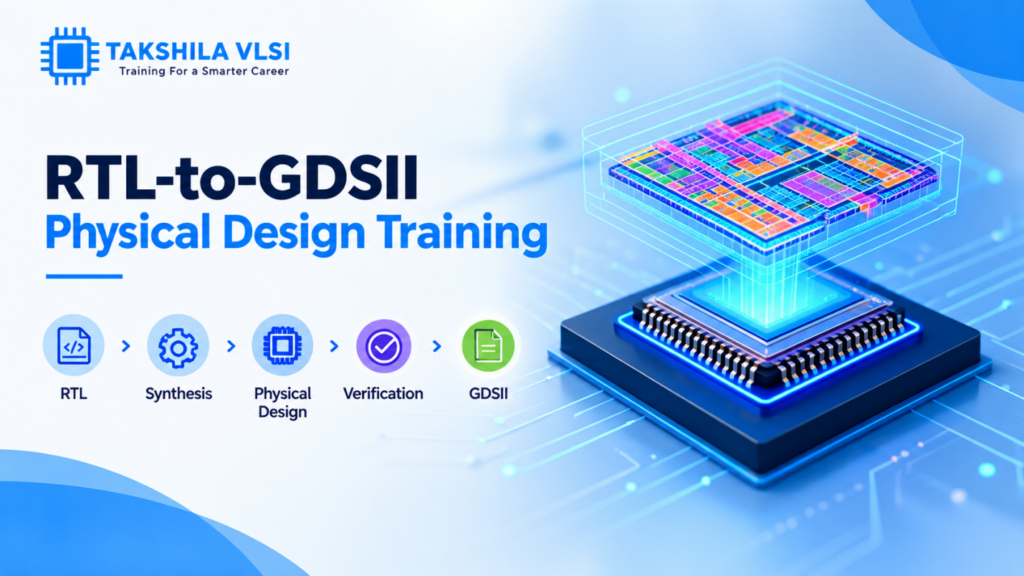
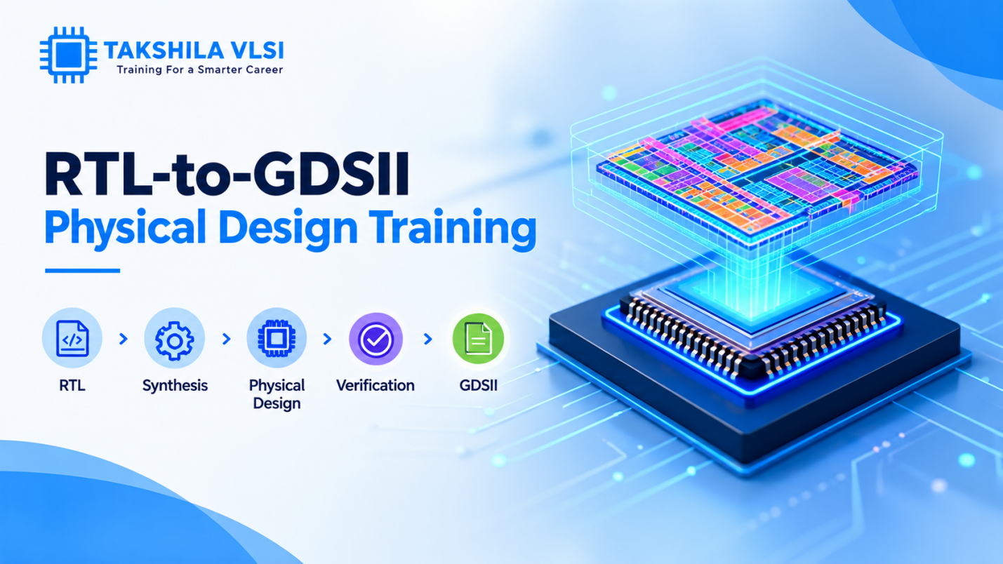
RTL-to-GDSII is the phrase you will hear repeated constantly once you start exploring physical design courses, and for good reason it describes the entire journey a chip design takes, from

If you have started exploring a career in VLSI, you have probably noticed that the field is not one single path but three distinct ones design, verification, and physical design

The semiconductor industry isn’t looking for paper knowledge or merely the names of training courses you attended. While certifications confirm completion of the curriculum, a candidate’s hands-on experience reflects their

Chip designers are pursuing chips with higher levels of complexity. While a chip can execute more instructions and functions and even reduce its power consumption. As it is becoming more

It’s often an overwhelming decision for BTech students pursuing the VLSI career path, specifically with Electrical Engineering, Electronics and Communication Engineering, or the equivalent backgrounds to choose the right field.