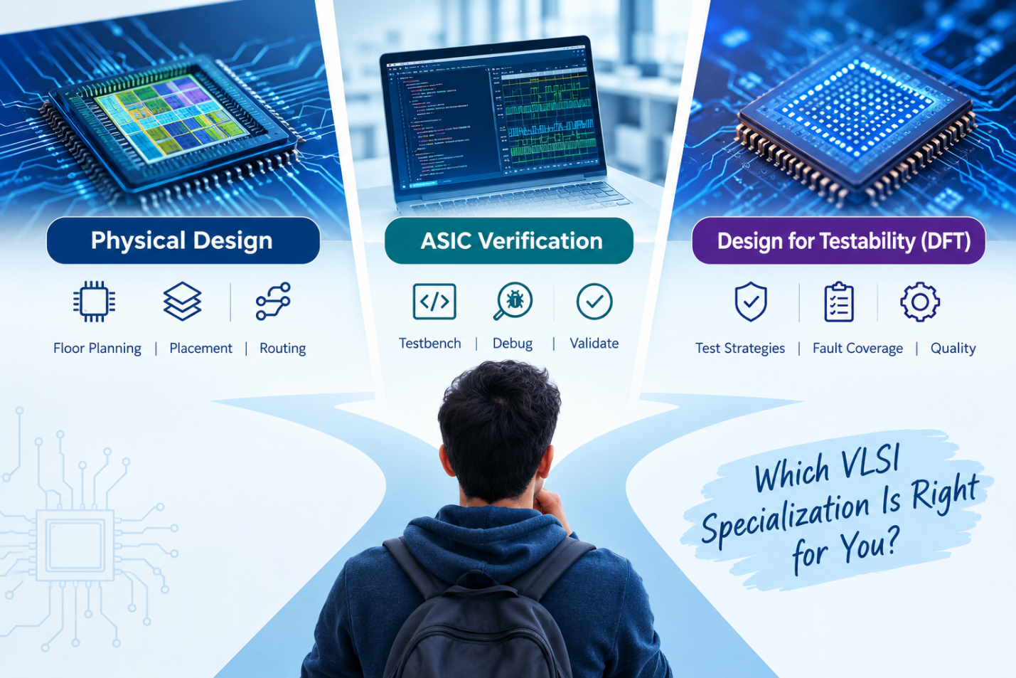
It’s often an overwhelming decision for BTech students pursuing the VLSI career path, specifically with Electrical Engineering, Electronics and Communication Engineering, or the equivalent backgrounds to choose the right field. Some of the most popular choices are the challenging fields like physical design, ASIC verification and Design for Testability(DFT).
So, right VLSI specialization after BTech is determined by your technical inclinations, technical expertise as well as what you aspire to in your professional journey. Following is a comparison of three major domains mentioned above to make your decision.
Understanding Your VLSI Career Options
When opting for VLSI career specialization, it should be a domain aligned with your passion for chip design, verification, testing or implementation. It is crucial to grasp the overview of each specialization, prior to choosing your field.
Physical Design
Physical Design is translating an electronic circuit into a blueprint that can be fabricated as a chip. Major steps include floor planning, placing, clock tree synthesis, routing, timing analysis, and physical verification.
Students who love problem solving, chip implementation, and working with EDA tools might opt for physical design careers.
While comparing physical design vs verification, Physical Design revolves around how a chip is physically laid, on the contrary, Verification is to confirm if the design is performing as specified.
ASIC Verification
ASIC Verification This field takes care of whether the chip that we designed functions the way we expected or not. Verification engineers use testbench languages and methodologies like Verilog, System Verilog and UVM to build and run a testbench.
If you enjoy playing with code, finding bugs, logical problems and dissecting complicated digital design, this field might be what you’re looking for. In verification, you get the chance to know and work with different streams that develop the chip.
If you like coding, and enjoy functional tests to ensure that your design is working as it is required, then verification can be a good candidate for you.
Design for Testability (DFT)
DFT is a niche in the VLSI design cycle which works to address the issue of easy testing of semiconductor devices for manufacturing flaws. With growing complexity in designing Chips, easy testing is one of the primary needs of semiconductor technology. Students specializing in this field learns about techniques and factors involved in making the quality of an integrated circuit better and testing it more efficient.
In contrast to DFT vs Physical Design, where The primary distinction here is the kind of work you do.
Which Domain Is the Best for Freshers?
There isn’t a specific best VLSI domain for Freshers and it depends upon the interests of the individual.
Select the Physical Design track if you want:
- To enjoy chip implementation and optimization.
- To dive into timing, routing, and physical verification.
- To work in the physical design tools and design flow space.
Select ASIC Verification if:
- You have a preference to code & debug.
- You have some interest in digital electronics.
- You enjoy to find out any design failure and test its functionality.
Select DFT if you:
- want to work in the field of chips and their quality.
- Like to know the manufacturing errors.
- Want to master an important sector in the SoC design.
A VLSI Career Path for ECE Students
A good VLSI career path for ECE students includes learning semiconductor basics and, then to develop strong domain specific skills. New graduates should concentrate on theory as well as on the hands-on experience.
The best VLSI domain selection guide is the one that takes into account your degree subject, interest in programming, interests and career choice. You can also identify a VLSI branch which you find best by working on projects in that domain and using the widely used VLSI tools.
How to Choose the Right Specialization
If considering for a VLSI specialisation for beginners, it is prudent to understand the concepts across various domains and then decide. Attend demonstration classes, analyse the course content and identify the practical implementation skills. The hands-on training is especially important, for it help students to relate theory and apply them in real design flows.
Conclusion
In the competitive world of semiconductors, an effective choice between Physical Design, ASIC Verification and DFT is critical for a strong career building among the career-oriented professionals. Everything must solely depend on the individuals’ inclinations, abilities and ambitions for the entire career prospect development.
Takshila VLSI is imparting various job-oriented training courses covering all the vital three branches that make all the trainees capable to possess hands on the industrial requirements of Physical Design, ASIC Verification and Design for Testability with best trainer supported teaching, lab practical exposure, high-end EDA tools facility, mock interviews support and placement assistant support to develop a solid career among all the budding professionals of VLSI development careers.