For most of the last two decades, chip designers had a fairly straightforward playbook: shrink the transistor, cram more logic onto one piece of silicon, and let the process node do the heavy lifting. That playbook is running out of pages. As nodes push past 5nm and toward 3nm and below, the cost of building one giant monolithic die keeps climbing, yields keep getting harder to hold onto, and the reticle itself puts a hard ceiling on how big a single chip can physically be. This is exactly why die-to-die interconnects have moved from a niche research topic to one of the most talked-about areas in VLSI over the past few years, and why any engineer building a career in physical design or SoC architecture needs to understand how they work.
What Exactly Is a Die-to-Die Interconnect
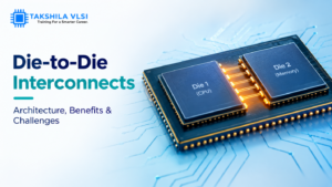
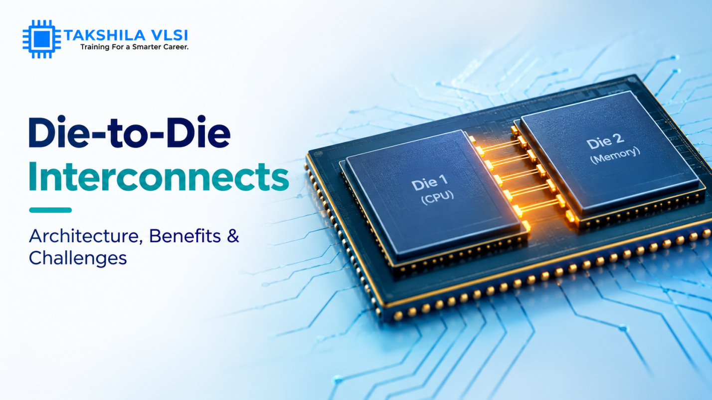
At its simplest, a die-to-die interconnect is the physical and electrical link that lets two or more separately manufactured silicon dies talk to each other as if they were one chip. Instead of building a compute core, memory controller, I/O block and analog front-end all on a single monolithic die, designers split these functions into smaller dies called chiplets, and then reconnect them inside one package using die-to-die connectivity. Done well, the connection is fast enough and power-efficient enough that the rest of the system barely notices it isn’t looking at a single piece of silicon.
Why the Industry Moved Toward Chiplets
There are three pressures pushing the industry in this direction. The first is yield. A large monolithic die has a much higher chance of containing a defect somewhere on its surface, and one small manufacturing flaw can scrap the entire chip. Break that same design into four or five smaller chiplets, and a defect only takes out one small piece, which is far cheaper to discard and replace. The second pressure is the reticle limit itself; lithography tools can only expose a fixed maximum area in a single pass, so once a design’s logic requirements exceed that area, splitting into multiple dies isn’t optional anymore. The third is economic flexibility. Not every block in a modern SoC benefits from the newest, most expensive process node, so chiplets let a company mix nodes within a single package instead of paying premium prices for parts of the design that don’t need it.
This is also the same shift driving the industry toward advanced packaging more broadly, from 2.5D and 3D integration to heterogeneous assembly, which we cover in more depth in Why Advanced Packaging Is Becoming a Must-Know Skill for Future VLSI Engineers. Die-to-die interconnects are really the connective layer that makes that entire packaging strategy work.
The Architecture Behind the Connection
A die-to-die interconnect is usually described in two layers, much like a networking stack. The physical layer, or PHY, handles the raw electrical signaling: the bumps, the micro-bumps or hybrid bonds that physically join the dies, the drivers and receivers, and the equalization needed to push a clean signal across a very short but electrically tricky path. Above that sits the protocol layer, which packages data into a format the receiving die can understand, handles flow control, and often tunnels standard protocols like PCIe or CXL across the link so that software above it doesn’t need to know or care that a die boundary even exists.
Two broad approaches show up here. Parallel, short-reach interfaces run wide buses at relatively lower per-pin speeds across very short distances, which is the approach used inside a single package where dies sit close together on an interposer or substrate. Serial, longer-reach interfaces trade wire count for speed per pin and are used when dies are farther apart or when the package uses a simpler substrate. The right choice depends on the bump pitch the packaging technology can achieve, the power budget available, and how much bandwidth the two dies actually need to exchange.
Universal Chiplet Interconnect Express and Why It Matters
For years, every company building chiplet-based products was more or less inventing its own die-to-die interconnect, which meant a chiplet from one vendor almost never worked with a die from another. Universal Chiplet Interconnect Express (UCIe) was created to fix exactly that problem. It defines a standardized PHY and protocol stack specifically for die-to-die communication, covering both the tight, high-bandwidth links used within a package and longer-reach links across a substrate, and it explicitly targets an open chiplet ecosystem where dies from different vendors can be assembled into a single working package. For a VLSI engineer, understanding UCIe is quickly becoming as relevant as understanding PCIe or DDR was a decade ago.
Where This Shows Up in a VLSI Engineer’s Day-to-Day Work
Working with die-to-die interconnects touches several disciplines at once, which is exactly why the topic comes up so often once you move past entry-level physical design work. It is worth getting comfortable with:
- Signal integrity analysis across a die boundary
- Power delivery network design spanning multiple dies
- Thermal coupling between neighbouring dies in one package
- Known-good-die testing before assembly
- Package co-design alongside floorplanning and routing
The Real Benefits
The payoff for getting a die-to-die interconnect right is significant. Smaller dies are cheaper to manufacture and easier to keep at high yield. Design teams can reuse a proven chiplet across multiple products instead of redesigning it from scratch every time, which shortens time to market considerably. Different chiplets can be built on whichever process node genuinely benefits them, rather than forcing an entire SoC onto one expensive node. And because chiplets are smaller, individual pieces can be tested before assembly, catching defective parts before they get bonded into an expensive final package.
The Challenges Engineers Actually Face
None of this comes free. Signal integrity across a die-to-die link is genuinely difficult; the interconnects operate at very high speeds across a boundary that introduces impedance discontinuities, and even small variations in bump height or substrate warpage can degrade the signal. Power delivery is another headache, since a package now needs to distribute power cleanly across multiple dies rather than one continuous plane. Thermal management gets harder too, because heat generated by one die can affect a neighbouring die in ways that don’t exist in a monolithic design. Testing known-good-die before assembly is essential, since a single bad die can waste an entire multi-die package. Latency across the interconnect also has to be tightly managed, and the EDA tooling and methodology for multi-die design is still maturing, so teams often have to stitch together flows across floorplanning, package co-design, and signal integrity analysis in ways a single-die project never required.
Conclusion
Chiplet-based design is not a passing trend; it’s becoming the default approach for high-performance computing, AI accelerators, and networking silicon. Physical design engineers who understand die-to-die interconnect architecture, signal integrity at the package level, and standards like UCIe are positioning themselves for the roles that leading semiconductor companies are actively hiring for right now.
Takshila VLSI trains students and working professionals on exactly these industry-relevant modules, with hands-on physical design and ASIC verification training backed by expert instructors, lab access to industry-standard EDA tools, project work, and placement assistance, so that engineers are ready for the multi-die, chiplet-based designs shaping the future of the semiconductor industry.