Physical design continues to be one of the most stable and well-paid career tracks within VLSI, and as chips get denser, faster, and more power-constrained, the demand for engineers who understand the RTL-to-GDSII flow has only grown. If becoming a physical design engineer is on your radar for 2026, here is a realistic, step-by-step look at what the journey actually involves from the fundamentals you need first, to the training path that gets you interview-ready.
Start With a Strong Grip on the Fundamentals
Before touching any EDA tool, a physical design engineer needs a solid understanding of digital electronics and CMOS fundamentals how transistors behave, what standard cells are, and how a gate-level netlist relates to an actual silicon layout. Alongside this, a working knowledge of basic Linux commands and scripting (particularly Tcl) is essential, since almost every tool in this domain is operated through the command line and custom scripts rather than a simple graphical interface. Skipping this foundation and jumping straight into tool training often leads to memorised steps without real understanding, which becomes obvious the moment an interviewer asks “why” instead of “how.”
Understand the Complete RTL-to-GDSII Flow
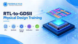
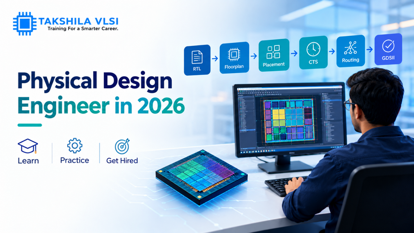
Physical design is a sequence of interconnected stages, and 2026’s hiring managers expect candidates to understand the flow as a whole, not just isolated pieces. This includes floorplanning, where the overall chip layout and macro placement are decided; power planning, which ensures the design has a reliable power delivery network; placement, where standard cells are positioned; clock tree synthesis, which distributes the clock signal with minimal skew; and routing, which connects everything together. Static timing analysis and physical verification (DRC and LVS) run throughout this flow, checking that the design meets its timing, power, and manufacturing requirements at every stage. A training path that treats these as separate, unrelated topics rather than a connected flow leaves a real gap in your practical understanding.
Get Genuinely Hands-On With Industry-Standard Tools
Reading about floorplanning is not the same as running it yourself, debugging a failed clock tree, or figuring out why a design is not meeting timing. In 2026, the industry expects familiarity with tools such as Cadence Innovus or Synopsys ICC2 for place-and-route, PrimeTime for static timing analysis, and Calibre for physical verification. The single most important thing to look for in a training program is individual, hands-on lab access not shared demonstrations so you build the muscle memory of actually running a design from floorplan to final GDSII on your own.
Work on At Least One Complete, Realistic Project
Employers consistently value candidates who can talk through a project in depth over those who can only recite theory. A meaningful training path should include at least one end-to-end project where you take a design through the full flow, hit realistic problems such as congestion, timing violations, or DRC errors, and work through fixing them. This project becomes your strongest talking point in interviews something you can explain confidently, defend your decisions on, and use to demonstrate genuine problem-solving rather than memorised steps.
Stay Aware of Where the Technology Is Heading
As of 2026, the industry is in active transition from FinFET to Gate-All-Around (GAA) transistor architectures at the leading edge, and while most entry-level roles will still work extensively with mature FinFET nodes, being aware of how GAA changes physical design considerations such as device modelling and parasitic effects signals to interviewers that you are keeping up with where the field is going, not just where it has been.
Build Strong Debugging and Analytical Habits
A large part of a physical design engineer’s actual job is debugging figuring out why a design is not converging on timing, why routing congestion keeps appearing in the same region, or why a DRC check keeps failing. This is a skill built through repeated hands-on practice and mentorship, not something that can be picked up from theory alone. Look for training that deliberately introduces you to realistic problems and guides you through the debugging process rather than only ever showing you successful runs.
Prepare Specifically for Physical Design Interviews
Physical design interviews tend to focus heavily on scenario-based questions “what would you do if your design is not meeting hold time after CTS?” being a classic example. Beyond technical concepts, interviewers assess how you reason through a problem. A good training path includes structured interview preparation, mock technical rounds, and guidance on how to present your project confidently, since this is often what separates two similarly skilled candidates.
Build a Habit of Reading Documentation and Release Notes
Tools and technology nodes evolve constantly, and engineers who make a habit of reading tool documentation, release notes, and industry articles tend to adapt faster when their company adopts a new tool version or process node. This habit is rarely taught explicitly in any course, but building it early even during training, by reading the manual for a feature before asking a mentor about it pays off steadily throughout your career.
Your Path Forward
Becoming a physical design engineer in 2026 is entirely achievable with the right combination of fundamentals, genuine hands-on tool experience, and real project work but the training path you choose makes all the difference. At Takshila Institute of VLSI Technologies, our physical design program is built around the complete RTL-to-GDSII flow, individual access to industry-standard EDA tools, and dedicated interview preparation. Check our course calendar to find the next batch and take a structured step toward your physical design career.