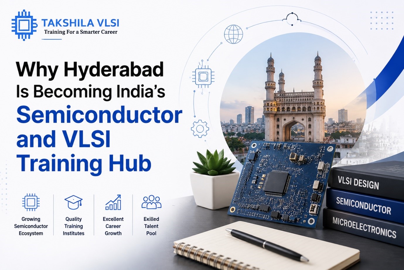
India’s chip industry has witnessed explosive growth. India has jumped light years in a few years and has become one of the preferred destinations for youngsters in terms of VLSI design jobs and seeking VLSI courses at the best training institutions. The investments, both public and private, into this sector; the globally renowned silicon giant’s presence; and top VLSI training and educational facilities have turned Hyderabad into an attractive place.
If you want to be involved in the semiconductor sector, knowing the reasons why Hyderabad has become a VLSI training hub in India might help you make the right career decision.
Hyderabad’s Growing Semiconductor Ecosystem
An extremely dominant part of this flourishing cityscape is the stellar Hyderabad semiconductor industry growth. Several government interventions like technology parks and major multinational semiconductor manufacturers have positioned the city as a hub for electronics and chip design. This, coupled with increasing numbers of companies setting up their R&D centres, has led to a spurt in demand for experienced VLSI professionals.
Access to Industry-Oriented Training
The best VLSI training institutes in Hyderabad aim to educate students with skills that meet real-time industry needs. Students will learn through live projects, not merely through theoretical knowledge, exposure to real-time design practices, and also advanced EDA tools.
Typical contents of modern VLSI courses in Hyderabad:
- Physical Design
- ASIC Verification
- Analogue Layout Design
- Design For Test (DFT)
- RTL Coding & FPGA Design
- Analog circuit Design
Strong Demand for Skilled Engineers
The semiconductor companies (chip design, fab companies) are expanding their footprint, resulting in numerous semiconductor career opportunities in Hyderabad. Employers are looking for students with the required industry experience for the following areas: backend design, verification & physical design. Usually, these students stand out as they receive 100% hands-on learning along with in-depth exposure to the full design cycle.
Why Students Choose Hyderabad for VLSI Learning
Reasons to choose Hyderabad for semiconductor education:-
- Availability of top VLSI institutes in Hyderabad
- Experienced trainers from the industry
- Modern EDA tools are available
- Project-based real-time learning
- Online, offline, and weekend batches are available
- Great Placement Assistance
- Increasing no. Of semiconductor employers in the network
Bright Future for the Semiconductor Industry
The future of the semiconductor industry in India is exceptionally bright, given the continuous investment flowing in with chip manufacturing, semiconductor design services, automotive, AI hardware, IoT, and communication systems gaining momentum in India. As more such large players are expanding, the demand for qualified VLSI engineers will continue to rise. Those who are focusing on learning now will surely find an edge in the next few years.
Conclusion
By integrating industry growth with high-quality technical training, Hyderabad has turned into one of the most potent places for semiconductor education. With expert trainers, hands-on lab experiences, industry-grade EDA tools, flexible modes of learning, and active placement assistance, institutes such as Takshila VLSI enable students to develop skills that are most sought after by employers in the industry. Enrolling in a professional VLSI course either as a fresher or a working professional seeking a skills upgrade will pave the way for a career in India’s booming semiconductor industry. In the race to seal Bangalore’s future as the numero uno semiconductor city in the nation, the decision to enrol at a VLSI training centre now could lay the path to a career in VLSI design or chip engineering.
FAQ
1. Why is Hyderabad becoming a VLSI training hub in India?
Hyderabad is becoming a VLSI training hub due to semiconductor industry growth, investments, multinational semiconductor companies, and top VLSI training facilities.
2. Why is Hyderabad important for the semiconductor industry?
Government interventions, technology parks, semiconductor manufacturers, and growing R&D centres have strengthened Hyderabad’s semiconductor ecosystem.
3. What do VLSI training institutes in Hyderabad offer?
They offer industry-oriented training through live projects, real-time design practices, and advanced EDA tools.
4. What topics are covered in modern VLSI courses in Hyderabad?
Courses typically cover Physical Design, ASIC Verification, Analogue Layout Design, DFT, RTL Coding, FPGA Design, and Analog Circuit Design.
5. What VLSI career opportunities are available in Hyderabad?
Growing semiconductor companies are creating opportunities in areas such as backend design, verification, and physical design.
6. Why do students choose Hyderabad for VLSI learning?
Students choose Hyderabad for its top VLSI institutes, experienced trainers, modern EDA tools, project-based learning, flexible batches, and placement assistance.
7. What is the future of the semiconductor industry in India?
The future is bright, with growing investment in chip manufacturing, semiconductor design, automotive, AI hardware, IoT, and communication systems.
8. How can VLSI training in Hyderabad help students build their careers?
Professional VLSI training provides hands-on lab experience, industry-grade EDA tools, expert training, and placement assistance to develop industry-ready skills.