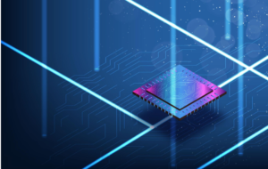
Entering the world of VLSI can be daunting for many freshers. The semiconductor industry is vast, offering numerous opportunities, and is constantly evolving. It is also highly technical, making it challenging for beginners to know where to start. However, the fact is that it’s effortless: given the right learning approach, the right learning path, and consistent practice, a person with a strong electronics background can develop into a skilled VLSI professional. Whether your objective is to work on chip design, verification, layout or cutting-edge fabrication technologies, the journey starts with clarity. And this clarity is precisely what a well-defined roadmap provides – one that takes you from your first step to being job-ready.
1. Understanding the VLSI Industry Before You Begin
The first step in your journey is getting a clear view of the core responsibilities, job roles, and growth opportunities within the domain. Today, millions of aspiring engineers search for a defined VLSI career roadmap, because knowing “what to learn” and “why it matters” prevents confusion and saves years of effort. The VLSI ecosystem covers RTL design, verification, analog design, physical design, testing, and EDA automation. Each path offers strong career stability, global relevance, and long-term growth. Among them, physical design stands out as a high-demand specialization with strong hiring needs worldwide.
2. Why Physical Design Is a High-Growth Career Path
Once you’ve read all the VLSI domains, it is noticeable that the demand for a Physical design engineer is always increasing because of the advancement in SoCs, AI chips, EV, and cloud infrastructure. Physical design is responsible for mapping RTL logic into the actual design of the silicon, making it one of the most critical stages in chip design. This job role requires precision, problem-solving, knowledge of timing closure, and good expertise with tools. Candidates who master these technical elements often enter high-value positions with strong long-term career security.
3. First Steps for Beginners: Building the Right Foundation
Every beginner needs a structured starting point, which is why new learners often look for the perfect VLSI fresher guide. Before diving deep, ensure your fundamentals in CMOS, digital electronics, Verilog, and logic design are strong. These basics serve as the foundation for everything you will learn later. Even if you are going to specialize in physical design, you still need to understand well combinational/sequential circuits, timing ideas and behavior of devices. Without this foundation, advanced tools and flows may be confusing.
4. Step-By-Step Learning Path for VLSI Success
As you move forward, it’s essential to maintain a systematic approach rather than jumping randomly between subjects. This is where a well-defined set of VLSI training steps becomes extremely important. Start with Verilog and progress to synthesis concepts, learn how timing constraints work and then slowly progress into place and route flows. Understanding timing closure, STA, and power optimization sets you up for industry-level design challenges. With each stage, your skills become keener and more relevant to industry expectations.
5. Entering the Job Market with Strong Skills and Confidence
After learning the required tools, design flows, and timing basics, you can start exploring internships and projects that interest you. Once you are well in the basics and have added some exposure of a project, then you can confidently search for VLSI jobs in different domains like physical design, verification, layout, RTL etc. Hiring teams are always looking for those learners who know real-world challenges and the workflow of the tool rather than theories.
6. Mastering Tools, Flows, and Industry Readiness
Beyond conceptual clarity, mastering Physical design flow, learning advanced EDA workflows, practicing real-world constraints, and solving timing issues are essential skills. Hands-on skills become even stronger with structured VLSI tools training and consistent practice. As you get closer to interviews, focused VLSI placement guidance allows you to navigate practical questions, problem-solving scenarios, and domain-specific challenges with ease. Over time, your personalized VLSI learning plan becomes your strongest asset for growth.
Conclusion
Becoming a physical design engineer is not about learning everything; it’s about learning the right things, in the right order, with the right guidance. A roadmap eliminates confusion and creates confidence while helping freshers become skilled professionals ready to take the high-demand roles of the semiconductor world. If you’re ready to start this journey with formal training and industry-leading direction, takshila-vlsi.com is still here to support the betterment of any aspiring VLSI learner’s career.