Have you ever wondered how a large phone, laptop, or car runs on a simple silicon chip? You are not alone. Future engineers tend to wonder what exactly goes on within a semiconductor fab. The reality is that the process of transforming raw silicon into a working chip is both interesting and very accurate. The first step towards a career in VLSI or chip design is that you understand the semiconductor manufacturing process, in addition to having a dream. We are going to simplify and break down every stage in a beginner-friendly manner in this guide because you can clearly see the journey.
Understanding the Foundations: What Makes Semiconductor Manufacturing Special?
To grasp the VLSI manufacturing basics, you must understand that semiconductor fabrication is not like typical manufacturing. Each of the steps occurs in controlled conditions, on microscopic scales and at the nanometer scale. That is why the semiconductor cleanroom process is necessary; any dust particle can ruin a whole wafer.
To learn the basics of the semiconductor industry as a first-time reader, it should be noted that chips are not made; they are developed, created, in hundreds of processes, one layer at a time.
Step 1: Wafer Preparation – The Beginning of the Chip Journey
Pure silicon serves as the starting material for the chip manufacturing guide. Sand is purified, smelted, and moulded into a rod of long crystal, which is known as an ingot. This ingot is cut into fine wafers. Any disorders in a quality semiconductor process flow are heavily dependent on a smooth, polished wafer, and any slight issue is likely to cause loss of yield.
Step 2: Oxidation – Building the First Protective Layer
Oxidation forms a thin silicon dioxide layer on the wafer surface. This insulating layer plays a major role in the semiconductor manufacturing process because it protects components, supports transistor formation, and acts as a base for upcoming layers. Mastering these early steps helps you grasp deeper VLSI manufacturing basics later.
Step 3: Photolithography – The Heart of Chip Fabrication
This stage combines optics, chemistry, and engineering skills. The wafer is coated with photoresist and exposed to UV light through a mask, a pattern of circuits.
These are known as semiconductor lithography steps, and they determine transistor size, density, and overall chip performance.
It is repeated many times to produce many circuit layers that compose photolithography, one of the most important steps in the semiconductor manufacturing process and the chip manufacturing guide.
Step 4: Etching – Removing Unwanted Material
After lithography forms the desired pattern on the wafer, the next stage is etching. In this step, all unexposed or unwanted areas are removed to reveal the actual circuit layout. Etching can be performed through dry methods, which use plasma, or wet methods, which rely on chemical solutions. This process brings the patterns to life and shapes the circuits with precision, playing a crucial role in the accuracy of the overall semiconductor process flow and final chip performance.
Step 5: Deposition – Adding New Layers
Once etching is complete, the wafer moves into the deposition stage, where essential materials such as polysilicon, metals, and dielectric layers are added. Techniques like Chemical Vapor Deposition (CVD) and Physical Vapor Deposition (PVD) help form thin, uniform layers on the wafer surface. These layers are vital for building the different components of the circuit, ensuring every part of the chip manufacturing guide receives the correct material structure needed to function properly.
Step 6: Ion Implantation – Controlling Electrical Properties
Ion implantation is the next key step, where dopants, charged particles, are injected into specific areas of the wafer. This process modifies the electrical conductivity of those regions, allowing engineers to define how transistors will behave. Since transistor performance depends heavily on precise doping levels, ion implantation is central to the VLSI manufacturing basics. Without controlled implantation, transistors would not switch ON or OFF correctly, affecting the entire circuit’s reliability.
Step 7: CMP – Achieving a Perfectly Flat Surface
Chemical-Mechanical Polishing (CMP) is then used to make the wafer surface completely smooth. This polishing step removes unevenness and prepares the wafer for additional layers. A flat surface ensures proper alignment and stacking during the semiconductor process flow, as even a tiny bump can impact the circuit’s performance or cause defects in future layers.
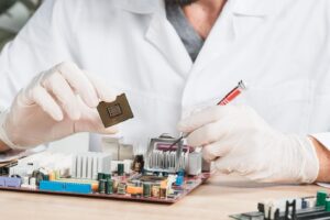
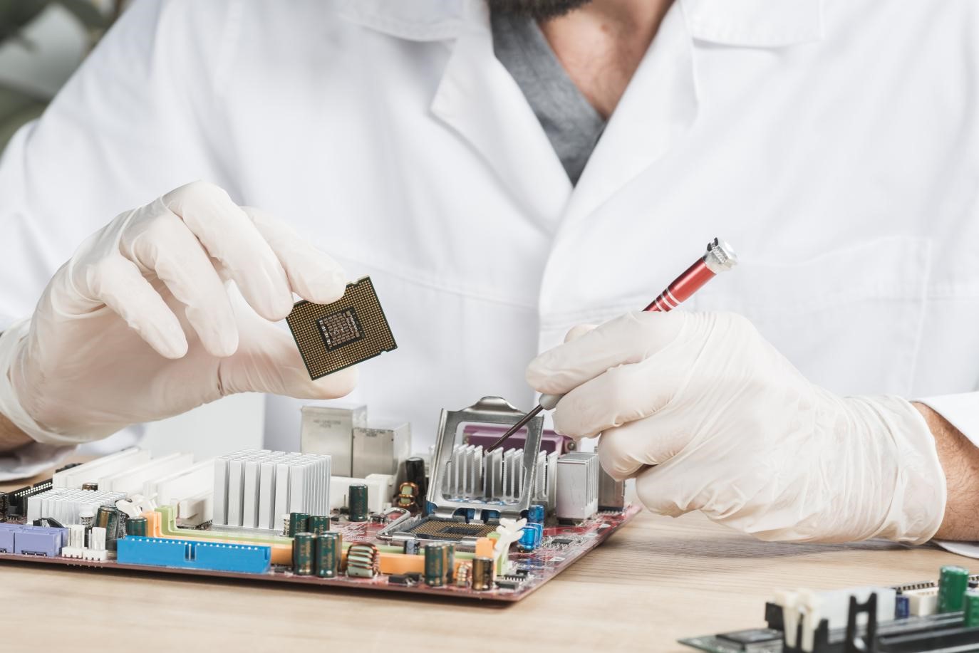
Step 8: Packaging & Testing – Bringing the Chip to Life
Once all fabrication steps are completed, the wafer is sliced into individual dies. Each die is carefully packaged to provide protection, manage heat, and enable electrical connections to the external world. After packaging, every chip undergoes rigorous testing to verify reliability, functionality, and performance. Testing is one of the most crucial phases of the chip manufacturing guide, especially in today’s high-density circuits, where even minor flaws can affect millions of devices.
Why Understanding Semiconductor Manufacturing Matters
Understanding the semiconductor manufacturing process gives you clarity on how engineering principles come together to form complex chips. It also builds a strong foundation for your VLSI manufacturing basics, accelerates learning in advanced subjects, and prepares you for fabrication, design, and testing roles.
The journey from silicon to system is complex, but incredibly rewarding for anyone passionate about VLSI.
Conclusion: Your First Step Toward a Semiconductor Career
Having observed the entire semiconductor process flow now, you can see more clearly how devices around you are created. Even with a good understanding of semiconductor industry basics, a clear understanding of the semiconductor lithography process and even familiarity with the semiconductor cleanroom process, you are already further along than most novices.
In case you are interested in practical training, semiconductor training at the industry level and real-world training, Takshila VLSI provides one of the most reputable semiconductor training programs to budding engineers. Starting with the concepts of fabrication to design-ready skills, they assist you in turning your passion into your career future.