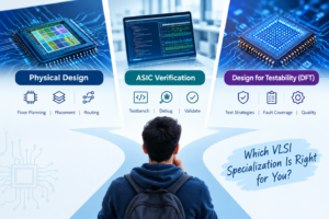
The constantly evolving semiconductor industry demands talented VLSI engineers in every segment, whether it be design, verification, or manufacturing. Enrolling on the appropriate VLSI design course will allow you the ability to provide you with robust foundational skills and prepare you prepared for future industry needs. The best VLSI chip design course generally includes practical exposure with lab sessions so as to give students the ability to acquire knowledge about the various aspects included in chip designing.
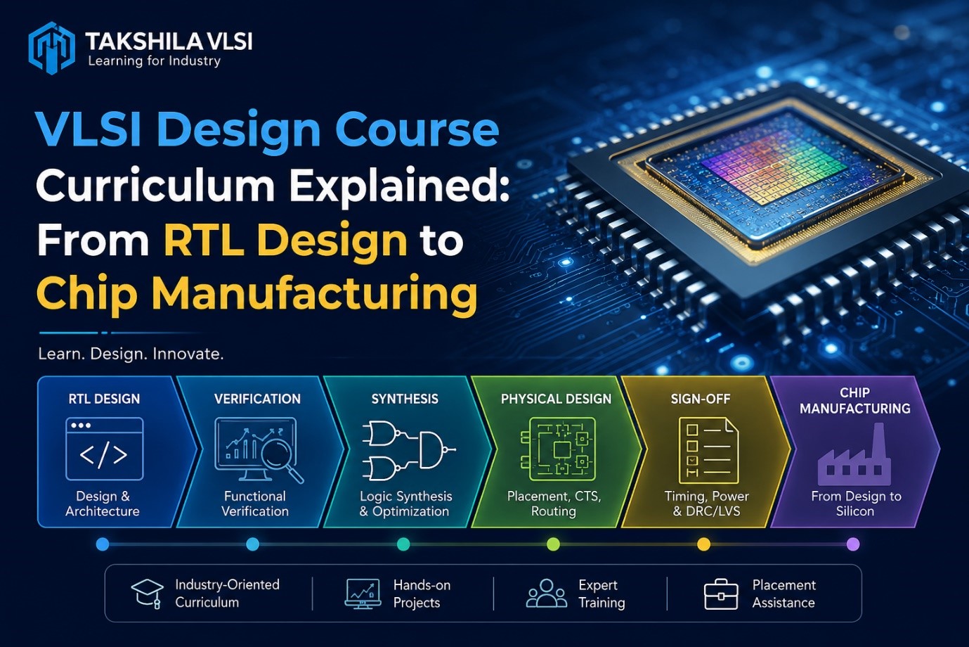
It includes the syllabus of a general VLSI design course to study, illustrating student development from RTL design to chip production stage, with appropriate technical expertise needed for a thriving career in semiconductor industries.
Understanding the VLSI Design Flow
Before touching upon the curriculum details, let us briefly learn about the VLSI design flow explained. Designing an IC necessitates numerous stages, and each of the stages needs expertise, and expertise needs appropriate tools.
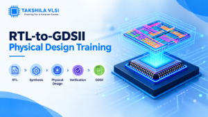
Below is a typical VLSI design flow:
- System specifications.
- RTL (Register-Transfer) Design.
- Functional verification.
- Logic synthesis.
- Physical design.
- Static Timing Analysis (STA).
- Physical verification.
- Tape-out.
- Chip fabrication and manufacturing.
- Chip testing and validation.
By taking an appropriately organized semiconductor chip design course students learn about each part by actually implementing it.
Module 1: RTL Design Fundamentals
VLSI design course curriculum’s first level deals with RTL(Register Transfer Level) design.
Here’s what students discover:
- Fundamentals of Digital electronics
- Verilog/SystemVerilog
- RTL coding standards
- How to write Finite State Machine (FSM) Designs
- Coding best practices
- FPGA implementation fundamentals
Students learn through in-depth RTL design training the way to engineer effective descriptions, which forms the basis on which complex microchips are built.
Module 2: Functional Verification
Following the development of RTL, the engineers have to make sure that the design functions as intended. This module is usually comprised of:
- Testbench development
- Simulation procedures
- UVM-based flow
- Assertion-based verification
- Debugging methods
- Coverage closure
Module 3: Logic Synthesis and Physical Design
After completion of verification, the code is then translated to gate-level logic by a tool referred to as synthesis.
Students will have hands-on experience in :
- Logic optimization
- Timing constraints
- Floor planning
- Power planning
- Placement
- Clock Tree Synthesis (CTS)
- Routing
Module 4: Timing Analysis and Physical Verification
The professional VLSI Design Course also talks of design quality before fabrication.
Topics will be on:
- Static timing analysis (STA)
- Signal integrity analysis
- IR drop analysis
- DRC rules and checks
- LVS verification
- Design optimization
Module 5: From Tape-Out to Chip Manufacturing
The last step in the RTL Design-to-chip manufacturing path brings students to the semiconductor manufacturing world.
Learners understand:
- Tape-out preparation
- Wafer fabrication
- Packaging
- Testing
- Yield improvement
- Production validation
Who Should Enroll?
This VLSI course for beginners and professionals has been structured for learners with different experiences and backgrounds.
These programs are designed to fit the needs of:
- Engineering students
- Recent graduates
- Electronics professionals
- Experienced engineers who want to advance their careers
- Career changers entering semiconductor design
Conclusion
The emphasis in the VLSI Design course programs ought not simply to be about making students experience theory – they have to meet the genuine business objectives and difficulties through theory with hands-on learning, experienced coaches and project-based guidance. The VLSI Design courses are produced keeping this point in mind and make learners take up the whole scope of VLSI design courses from RTL design to semiconductor chip manufacturing process to assist them obtain the requisite in-depth technical proficiency required by the top multinational corporations that are associated with us.
With industry masters who direct the lessons to provide appropriate access to labs and other important hardware & tool utilization, supplemented by specialized situation help for graduates as well as those individuals currently working, Takshila stands apart as the place to assemble a fruitful VLSI design or semiconductor design career!