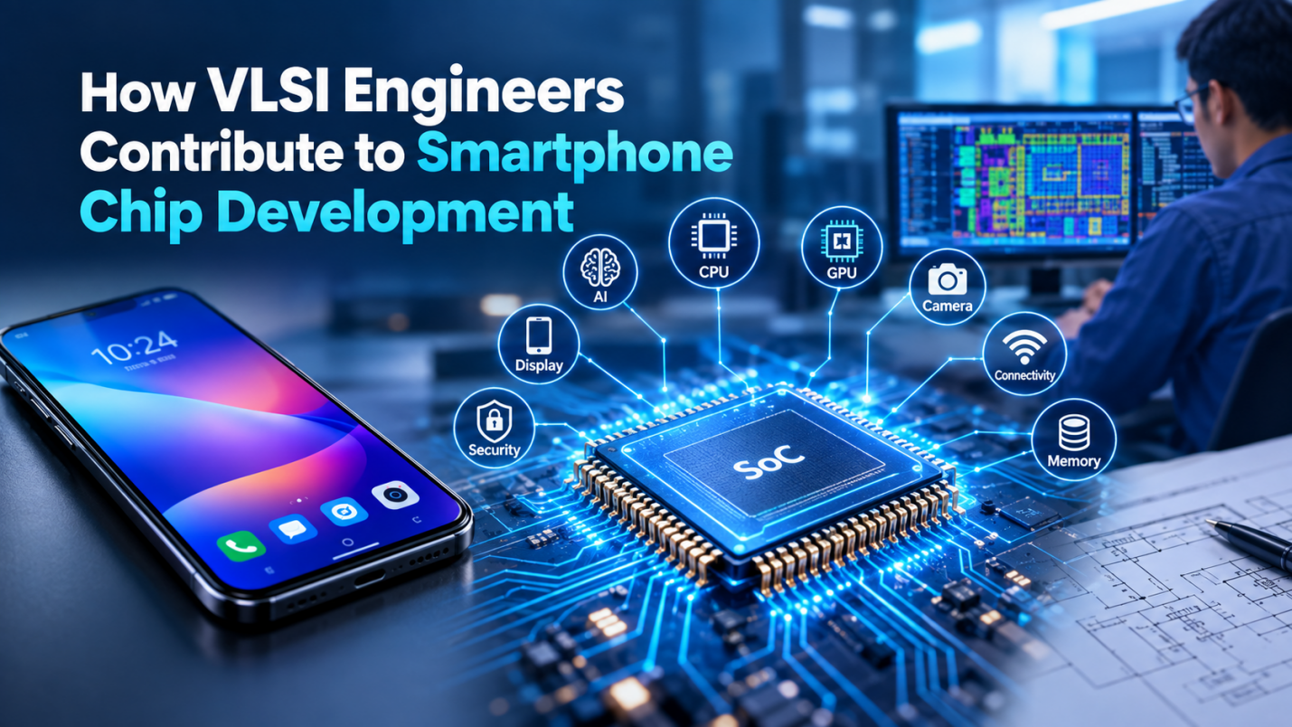
Smartphones have truly become powerful tools, capable of anything from professional quality photography, gaming to intelligent systems, to high tech communications. Behind all of these smart phones and applications is advanced technology of semiconductors.VLSI is an important element responsible for powering the mobile phones of the 21st century. The use of VLSI in smartphone chips enables more powerful, more efficient and smaller mobile phones. VLSI engineers work to assist in several chip development processes that help realize mobile phones, from design concept to silicon product.
Understanding Smartphone Chip Design
Smartphone chip designs are essentially highly complex, fully integrated circuits. Integrated circuits integrate diverse elements onto a very small silicon chip that form a part of a smartphone such as a processor, graphics chip, memory interfaces, communication circuits, etc. In general, modern smartphones utilize the system on a chip (SoC) design which integrates all such components. Chip design engineers under VLSI are engaged with design, verification, layout and testing, enabling modern smartphones to provide optimum performance for reduced power consumption.
The Role of VLSI Engineers in Mobile Technology
VLSI engineers in mobile technology participate in various fields of development like circuit designing, physical designing, verification, testing and layout designing etc depending upon their roles and profiles.
Their responsibilities may involve:
- Drawing digital and analog circuits.
- Proving and checking circuits.
- Making physical design (chip floor planning/placement and routing).
- Maximizing power, performance, and area of the design.
- Highlighting possible design pitfalls.
- Working closely with the testing engineers to manufacture and test the chip.
Mobile Processor Design and Performance Optimization
Chip development in mobile processor design is an enormous area. Mobile processors for smartphones have billions of computations to execute at very constrained power and thermal limits.
VLSI engineers assist in each section of a processor to maximize performance. They optimize the logical design, timing analyses, the physical implementation and the verification stages of a chip. Power optimization is one very large sector because a mobile phone runs on batteries. There must be adequate performance without over-consuming battery life.
Semiconductor Design for Smartphones
Semiconductor design for smart phone application chips involves many features which must be integrated into the small footprint of the smartphone. A single smart phone chip might support processing, graphics, wireless connectivity, cameras, security as well as numerous applications including artificial intelligence. Designing a chip of this nature requires tight design flow coordination and expertise among different designers such as: analog, digital, layout, verification and physical design.
The Importance of Mobile SoC Design
The design of a mobile SoC involves the fusion of various devices onto a single chip. A smart SoC design can result in a device with increased performance, smaller size and improved power economy.
A typical high-end smartphone SoC consists of CPU cores, GPUs, memory interfaces, communication interfaces and dedicated processing elements. All these blocks must be individually designed and interlinked in a system. This requires considerable VLSI knowledge.
Key VLSI Applications in Smartphones
Today’s Smartphones make great use of many VLSI applications. Some coreVLSI functionalities include:
- Mobile processing power
- Camera subsystem
- Wireless connectivity
- Display technologies
- Power management solution
- Audio processing block
- Security features (fingerprint etc.)
- Capabilities concerning artificial intelligence and machine learning
Conclusion
Opportunities in the semiconductor industry, due to growing needs in the field of smartphones are on the increase for professionals. Right from VLSI in Smartphone chips to development of advanced processors and SoCs, engineers are working at different levels. Building hands-on experience in the form of formal training is an excellent starting point for beginners aiming to work in the VLSI industry.
Takshila VLSI provides this opportunity in various forms to fresh graduates and working professionals in the forms of different training programs in areas like Physical Design, ASIC Verification, Analog Layout Design, Design for Test and Analog circuit Design.
Highly skilled trainers providing practical insights with comprehensive learning tools are also enabling students to land themselves in interesting opportunities by leveraging their career with well designed programs leading to placement at a reputed concern in this sector.