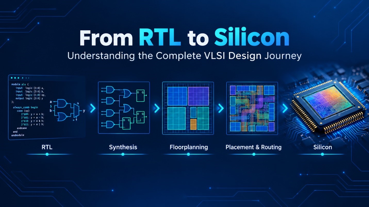
Every chip in your phone, laptop or car started as a plain-language specification. Somewhere between that document and the finished piece of silicon, thousands of decisions were made, checked, rechecked and sometimes thrown out. Understanding that path is the single most useful mental model a new VLSI engineer can have.
This article walks through the VLSI design flow from RTL to silicon, step by step, with a sense of where things tend to go wrong.
The big picture
People describe this in different ways: the RTL design flow, the semiconductor design process, the ASIC design flow, the chip development lifecycle. They’re all circling the same idea.
A chip doesn’t move through a straight line. It moves through a series of refinements, each one more concrete than the last. Roughly:
Specification → Architecture → RTL design → Verification → Synthesis → Physical design → Signoff → Tape-out → Fabrication → Testing and validation
Teams loop back constantly. A timing problem found in physical design may send you back to RTL. A bug found after fabrication may mean another revision. The flow is a guide, not a conveyor belt.
Step 1: Specification and architecture
Before any code, someone decides what the chip must do. How fast should it run? What’s the power budget? Which interfaces does it need? Architects explore options and settle on a high-level design, often built from blocks like processors, memory controllers and peripherals.
Mistakes here are the most expensive, because everything downstream builds on them. A wrong assumption about bandwidth, caught late, can force a redesign.
Step 2: RTL design
RTL, or register transfer level, describes how data moves between registers and what logic transforms it each clock cycle. Designers write it in Verilog, SystemVerilog or VHDL.
This is the stage most people picture when they imagine chip design. Good RTL is more than functional. It’s written with synthesis in mind: no accidental latches, clean clock and reset strategy, sensible pipelining and clear hierarchy. Writing hardware descriptions that merely simulate correctly isn’t enough. They have to become real circuits.
Step 3: Functional verification
Once RTL exists, verification engineers test it against the specification. They build testbenches, generate stimulus (often constrained-random), check outputs and measure coverage to see what’s been exercised.
Verification typically consumes the largest share of effort in a chip project, since fixing a bug after tape-out is extraordinarily costly. Techniques include simulation, assertions, formal verification and emulation for large designs. The goal isn’t proving the absence of bugs, which is impossible, but reducing risk to an acceptable level.
Step 4: Logic synthesis
Synthesis translates RTL into a gate-level netlist built from cells in a target technology library. The tool uses constraints, usually in SDC format, that describe clock frequencies, input and output delays, and exceptions.
Good constraints matter as much as good RTL. Under-constrained designs can look fine and fail in silicon. Over-constrained ones waste area and power. After synthesis, teams run equivalence checks to confirm the netlist still matches the RTL.
Step 5: Design for test insertion
Manufacturing isn’t perfect, and chips need ways to be checked for defects. DFT engineers insert scan chains, built-in self-test for memories and boundary scan structures. These add a bit of area, but without them, testing a complex chip economically would be nearly impossible.
Step 6: Physical design
Now the netlist becomes geometry. The main stages:
- Floorplanning: deciding where major blocks and I/O sit on the die.
- Power planning: building the grid that delivers power across the chip.
- Placement: positioning each standard cell.
- Clock tree synthesis: distributing the clock so it arrives at every flip-flop in a controlled way.
- Routing: connecting everything with metal layers.
- Timing closure: iterating until setup and hold requirements are met everywhere.
This phase blends engineering and craft. Congestion, IR drop, crosstalk and timing violations all compete for attention, and fixing one can worsen another.
Step 7: Physical verification and signoff
Before a design is sent to the foundry, it must pass a strict set of checks:
- Static timing analysis across multiple corners and modes
- Design rule checking (DRC) against the foundry’s manufacturing rules
- Layout vs schematic (LVS) to confirm the layout matches the intended circuit
- Power and IR drop analysis
- Electromigration and signal integrity checks
Signoff is the formal “we believe this will work” moment. Passing means the design meets every requirement the foundry and the project defined.
Step 8: Tape-out and fabrication
Tape-out is the point at which the final layout database, usually in GDSII or OASIS format, goes to the foundry. The term comes from the days when data was literally shipped on magnetic tape.
Fabrication then builds the chip layer by layer on silicon wafers. It takes weeks to months, and masks are costly, which is why teams verify so thoroughly beforehand.
Step 9: Packaging, testing and validation
Wafers are cut into dies, tested, packaged and tested again. Then comes post-silicon validation: engineers bring up the first chips in the lab, run real software on them, and compare behaviour against expectations. Issues discovered here can lead to a respin, or get handled through firmware workarounds where possible.
Where careers fit in this journey
Each step above is a job family. Architects, RTL designers, verification engineers, synthesis and timing specialists, DFT engineers, physical designers, signoff experts and validation engineers all contribute. Knowing the whole flow helps you pick a specialization and makes you a better teammate in whichever one you choose. A designer who understands physical design writes RTL that’s easier to implement. A verification engineer who understands timing reports better bugs.
Tips for learners
- Learn the flow end to end before specializing deeply.
- Take a small design, perhaps a simple counter or ALU, through every stage, even in a tutorial environment.
- Read timing reports regularly until they stop looking intimidating.
- Ask “what could go wrong here?” at every step. That question builds engineering judgment.
Closing thoughts
The path from RTL to silicon is long and full of checkpoints for good reason. Each stage catches problems that the next one can’t easily fix. Once you can picture the full journey, individual topics like STA, DFT or UVM stop feeling like separate subjects and start fitting into one coherent picture.
If you want to experience this flow on real tools rather than only read about it, the guided programs at Takshila VLSI take learners through the complete design cycle with hands-on projects.
Frequently asked questions
What does RTL stand for?
Register transfer level, a way of describing digital hardware by how data moves between registers.
How long does it take to design a chip?
It varies widely, from several months for a small block to a few years for a complex SoC.
What is tape-out?
The moment the finished design data is handed to the foundry for manufacturing.