Chip designers are pursuing chips with higher levels of complexity. While a chip can execute more instructions and functions and even reduce its power consumption. As it is becoming more difficult for standard scaling to work anymore due to transistor improvements, engineers seek alternative ways at lower levels, including the package design of numerous chips into single integrated units to enhance functionality. Thus, advanced packaging in VLSI is now a critical section to learn for budding and current VLSI engineers.
What Is Advanced Packaging in VLSI?
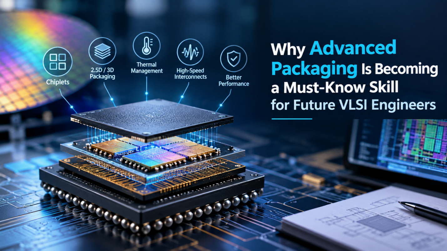
These innovative methodologies involve designing advanced packages that consolidate die, die, memory devices, etc, in one device, rather than just shielding them. Chipsets and advanced networks facilitate improved communication, enhance operational capacity, help with temperature controls, and boost the efficiency and operations of the overall product. Chiplets, extremely high-bandwidth connections, and integrated elements contribute to the overall new designs of modern chip technology, and the VLSI packaging technology can provide a better perspective for the design engineers toward the chip development process.
Why Semiconductor Packaging Skills Matter
No longer do we build chips based on individual circuits. Chip design is evolving to require us to know how the pieces are connected and behave once they’re built. Learning about semiconductor packaging offers a good way for professionals to get up to speed on many of these crucial issues, such as signal integrity, power, thermal, interconnect, and performance on the package. For a VLSI student or a fresher, knowledge of these topics will add to their expertise in physical design, analog layout, verification, and circuit design.
Understanding Advanced IC Packaging
With more advanced IC packaging, engineers can integrate a variety of technologies into a single device. This is illustrated by an application of chiplet-based design, in which individually manufactured dies can be integrated to form one integrated unit.
It is good to get familiar with:
- Die-to-die communication
- High-density interconnects
- Thermal handling
- Signal and power integrity
- Package-level testing
- Heterogeneous integration
The Rise of 2.5D and 3D Packaging
Another key technology developing today is 2.5D 3D packaging. These technologies allow for closer packaging of dies or components for possible gains in bandwidth, performance, and overall system integration. With the discussion of chip manufacturers no longer able to shrink feature sizes, these architectures are an increasingly important factor for engineers to be aware of in next-generation designs.
Packaging-Aware Design Is the Future
Early consideration for packaging is now a necessity in modern semiconductor development. With packaging-aware design, designers are pushed to see the implications of package performance on electrical, thermal, and physical design, which is why semiconductor engineering skills are expanding to include a knowledge of packaging technology. This is why students gaining an understanding of both fundamentals and design methods of packaging technologies will also have more knowledge in core VLSI.
How Future VLSI Engineers Can Prepare
Most effective in enhancing such skills would be practical structured training. Students should not only grasp the fundamentals of semiconductors but also be abreast of industry-based areas, EDA concepts, lab experiences and project-oriented learning.
At Takshila Institute of VLSI Technologies, the students can undertake special courses for VLSI under fields such as physical design, analog layout design, ASIC verification, DFT, Analog circuit design, and RTL coding and FPGA design. The focus is placed on practical learning, expert training, lab facilities and guidance, projects, and placement assistance.
Conclusion
As technology is changing the future of semiconductor design, packaging plays a major role as it is evolving as a significant element in the VLSI industry ecosystem. Understanding packaging in addition to design and verification helps engineer develop a better view of developing cutting-edge chips in modern days.
Takshila VLSI trains students on industry-based modules and prepares them for a semiconductor career in a realistic manner with expert instructors, hands-on learning experience, superior equipment, and placement services for emerging VLSI engineers.