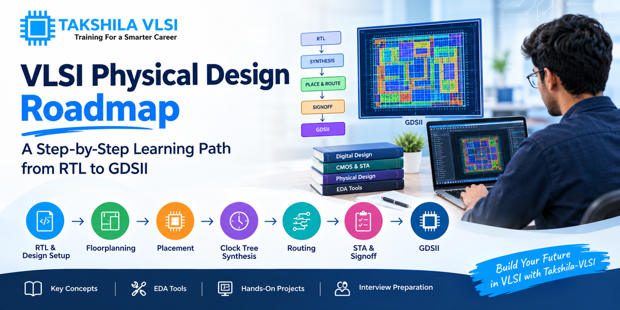
Ask ten physical design engineers how they got started and you will hear ten different stories. Some came from electronics, some from computer science, and a few switched from completely unrelated jobs. What they share is a habit: they learned the flow in order, practiced each stage on real designs, and only then moved to the next one.
This guide lays out that order. If you are a fresher wondering where to begin, or an engineer trying to build a physical design roadmap you can actually follow, you will find the prerequisites, the stages of the RTL-to-GDSII flow, the tools, the projects and the interview preparation in one place.
What Physical Design Actually Is
A chip starts as an idea, becomes RTL code, and is turned by synthesis into a netlist of logic gates. Physical design takes that netlist and decides where every gate sits on the silicon, how the wires connect them, and whether the finished layout meets the timing, power and manufacturing rules. The final output is a GDSII file, which is what goes to the foundry.
It is a job of trade-offs. A tighter placement shortens wires but can cause routing congestion. A faster clock needs more buffers, and buffers cost power. A good physical design engineer learns to balance these forces rather than chase a single number.
Prerequisites: What to Know Before You Start
You do not need to be an expert in everything, but a few foundations make the rest of the journey far easier.
- Digital electronics: logic gates, flip-flops, setup and hold concepts, and basic sequential circuits.
- CMOS basics: how an inverter works, delay, and why power and area matter.
- Basic Verilog: you do not have to write complex RTL, but you should be able to read a small module.
- Linux and scripting: nearly every EDA tool runs on Linux, and Tcl, Perl or Python scripts save hours of repeated work.
Spend three to four weeks on these if any of them feel shaky. Time spent here is repaid many times over when you start debugging timing reports.
The RTL-to-GDSII Flow, Stage by Stage
1. Synthesis and Design Setup
Before layout begins, you receive a netlist, timing constraints (SDC), library files and technology data. Learn what each of these contains. Most beginner mistakes at later stages trace back to a misunderstood constraint file or a missing library.
2. Floorplanning
Floorplanning sets the stage for everything else. You define the die size, place the macros and memories, plan the I/O pins and create the power grid. A poor floorplan cannot be rescued by clever routing later, which is why experienced engineers spend extra time here. Practice reading congestion maps and learn why macro orientation and spacing matter.
3. Placement
The tool now places the standard cells in rows. Your job is to guide it with sensible constraints, check utilization, and review timing and congestion after placement. You will also meet optimization steps such as buffering and cell sizing.
4. Clock Tree Synthesis (CTS)
A clock signal has to reach thousands of flip-flops at nearly the same moment. CTS builds a balanced network of buffers to make that happen. Study clock skew, insertion delay, useful skew and clock gating. This stage is where many learners first realise how closely timing and physical layout are linked.
5. Routing
Routing connects all the cells using metal layers. Global routing plans the paths, and detailed routing creates the actual wires. Expect to deal with design rule violations, crosstalk and antenna effects. Learning to read and fix these violations is a core skill.
6. Static Timing Analysis (STA) and Signoff
STA runs through the whole flow, not just at the end. You check setup and hold slack across corners and modes, fix violations, and confirm power integrity. Before tape-out, physical verification checks such as DRC and LVS confirm the layout follows foundry rules and matches the schematic intent.
If you are short on time, give STA the largest share of your attention. It appears in nearly every interview and in nearly every real project.
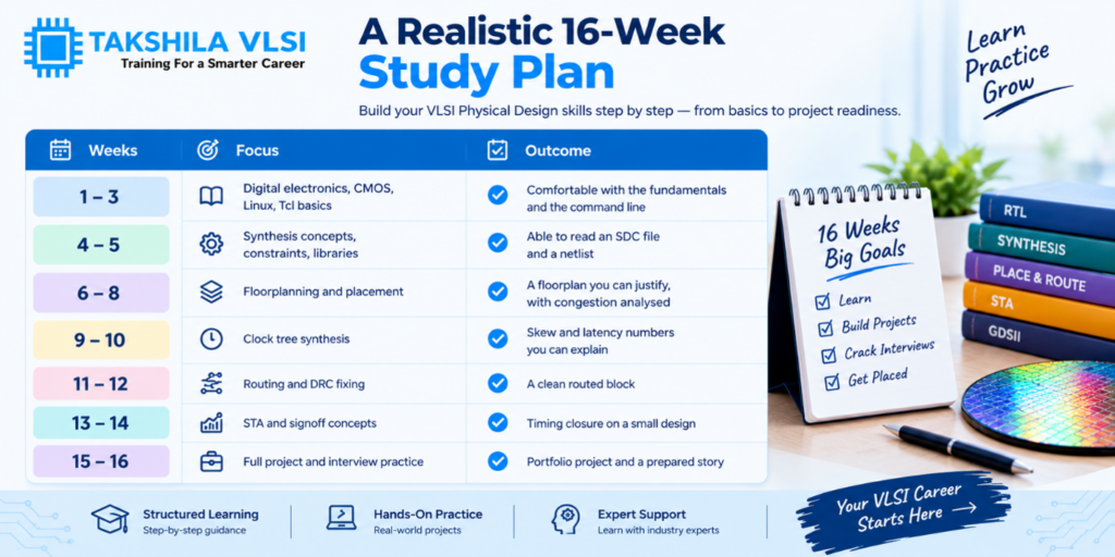
A Realistic 16-Week Study Plan
| Weeks | Focus | Outcome |
| 1-3 | Digital electronics, CMOS, Linux, Tcl basics | Comfortable with the fundamentals and the command line |
| 4-5 | Synthesis concepts, constraints, libraries | Able to read an SDC file and a netlist |
| 6-8 | Floorplanning and placement | A floorplan you can justify, with congestion analysed |
| 9-10 | Clock tree synthesis | Skew and latency numbers you can explain |
| 11-12 | Routing and DRC fixing | A clean routed block |
| 13-14 | STA and signoff concepts | Timing closure on a small design |
| 15-16 | Full project and interview practice | Portfolio project and a prepared story |
Treat the plan as a guide rather than a rule. If STA takes you five weeks instead of two, that is fine. Depth matters more than speed.
EDA Tools You Will Encounter
The industry relies on tools from Synopsys, Cadence and Siemens. Typical names include Fusion Compiler and IC Compiler II, Cadence Innovus, PrimeTime and Tempus for timing, and Calibre for physical verification. You will rarely get free access to all of them, so choose a training program that offers hands-on lab time. Reading about a tool is not the same as watching a timing report change after you fix a path.
Whichever tool you use, focus on the concepts underneath. Engineers who understand why a hold violation happens can move between tools with little trouble.
Hands-On Projects That Build Real Skill
- Small block, full flow: take a modest design such as a UART or a small RISC core through floorplanning, placement, CTS and routing.
- Timing closure exercise: start with a block that fails timing and document every change you make to fix it.
- Power grid study: compare two power grid strategies and report the IR-drop difference.
- Congestion analysis: change macro placement and record its effect on routing.
Write short notes on each project: what the problem was, what you tried, what worked and what did not. Interviewers love candidates who can explain a failed attempt.
Interview Preparation for Physical Design Roles
Interviews usually mix concept questions with scenario questions. Be ready for topics such as:
- What causes a setup violation and how would you fix it? How is a hold violation different?
- Why do we use useful skew, and what are its risks?
- How do you reduce congestion in a crowded region?
- What is the difference between global and detailed routing?
- How do on-chip variation and multiple corners affect timing signoff?
Practice answering aloud. Many candidates know the answer but struggle to explain it clearly in two minutes. Draw a quick diagram when it helps, and tie your answer to a project you actually worked on.
Common Mistakes to Avoid
- Jumping straight into tool commands without understanding the concept behind them.
- Skipping STA because it feels dry. It is the backbone of the role.
- Collecting certificates instead of building projects.
- Ignoring scripting. Automation is what separates a trainee from a productive engineer.
Where to Go from Here
Physical design rewards patience. The learners who succeed are rarely the fastest; they are the ones who keep returning to the same timing report until they understand every line of it. Follow the flow in order, practice each stage on real designs, and build one project you can talk about with confidence.
If you would like structured guidance, lab practice and mentoring along the way, explore the Physical Design course at Takshila Institute of VLSI Technologies and see how the curriculum maps to this roadmap.