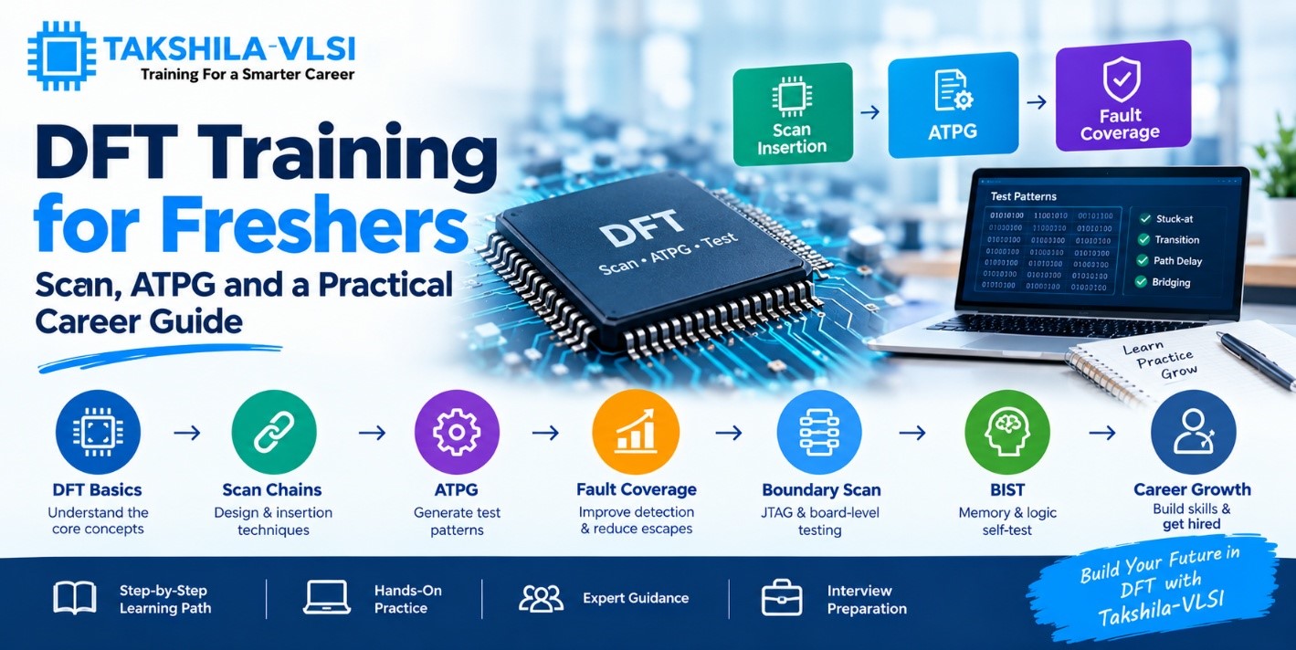
Every chip that leaves a factory must be tested, and testing a chip with billions of transistors is not as simple as switching it on. Without help built into the design itself, many defects would never be found. That built-in help is what Design for Testability, or DFT, is all about.
DFT is a smaller field than design or verification, which is exactly why many freshers find it attractive. Fewer people specialise in it, and every serious chip company needs it. This guide explains the core ideas, the skills to build and how to prepare for interviews.
What Is Design for Testability?
DFT means adding extra logic to a chip so that manufacturing defects can be detected quickly and cheaply. A fabricated chip may have a tiny short, an open connection or a weak transistor. DFT gives test equipment a way to control internal nodes and observe the results, even though those nodes are buried deep inside the chip.
Think of it as adding inspection windows to a building before it is constructed. Trying to cut windows afterwards is far more expensive.
Scan Chains and Scan Insertion
The most common DFT technique is scan design. Ordinary flip-flops are replaced with scan flip-flops that have an extra multiplexer at the input. In normal mode the chip works as designed. In test mode, the flip-flops link together into long shift registers called scan chains.
This lets a tester shift a known pattern into every flip-flop, apply one or more clock pulses, and shift the captured response out. In effect, the hard problem of testing sequential logic becomes a much easier combinational one.
What scan insertion involves
- Replacing normal flip-flops with scan-capable ones
- Stitching them into balanced chains, often grouped by clock domain
- Adding scan-enable, scan-in and scan-out connections
- Handling lockup latches and clock-domain crossings between chains
- Running design rule checks to confirm the design is scan-ready
Tools such as Synopsys DFT Compiler or Cadence Modus and Genus handle much of the insertion, but you must understand the choices behind each setting.
ATPG: Generating the Test Patterns
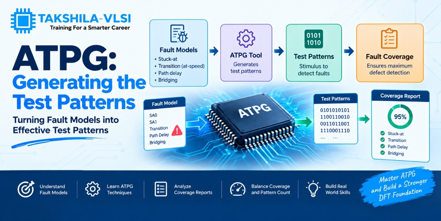
Once scan chains are in place, Automatic Test Pattern Generation (ATPG) tools create the patterns used to test the chip. The tool targets fault models, which are simplified descriptions of how a defect might behave.
| Fault model | What it represents |
| Stuck-at | A node permanently stuck at logic 0 or 1 |
| Transition (at-speed) | A node that switches too slowly, causing timing failures |
| Path delay | A complete path that is slower than the clock period allows |
| Bridging | Two nearby wires accidentally shorted together |
Stuck-at testing is the starting point, but modern chips also need at-speed tests, because many real defects only show up when the chip runs at full frequency.
Fault Coverage and Pattern Count
Fault coverage is the percentage of modelled faults that the patterns can detect. Higher coverage means fewer defective chips slip through. But every pattern costs tester time, and tester time costs money. DFT engineers constantly balance coverage against pattern count, and compression techniques help by reducing the data needed without losing detection.
Learn to read an ATPG report. Understanding why certain faults are untestable, such as those blocked by constants or by logic with no observation path, is a skill interviewers look for.
Boundary Scan, BIST and Other Techniques
- Boundary scan (JTAG, IEEE 1149.1): a standard way to test connections between chips on a board and to access on-chip debug features.
- Memory BIST: built-in self-test logic that tests on-chip memories, which take up a large share of chip area.
- Logic BIST: self-test for logic blocks, useful where external tester access is limited.
- Test compression: reduces test data volume and test time.
- IJTAG (IEEE 1687): a flexible method to reach internal test instruments.
You do not need to master all of these on day one. Start with scan and ATPG, then add boundary scan and memory BIST.
Skills to Build as a Fresher
- Strong digital design basics, especially sequential logic and timing
- Comfortable Verilog reading and simple RTL writing
- Understanding of STA, since scan introduces new timing paths to check
- Tcl or Python scripting for automating tool flows
- Patience for debugging simulation mismatches, which is a big part of the job
A Simple Learning Path
- Revise digital logic and learn the basics of fault models.
- Study scan design and manually trace how a scan flip-flop behaves in shift and capture modes.
- Insert scan into a small design using a tool and run design rule checks.
- Generate stuck-at and transition patterns and study the coverage report.
- Simulate the patterns with the netlist and debug any mismatch.
- Learn boundary scan and memory BIST concepts.
- Combine everything in one end-to-end mini project.
Career Scope in DFT
DFT engineers work in semiconductor companies, product firms and design service houses. Roles include DFT design engineer, ATPG engineer, test engineer and product engineer. Because DFT sits between design, physical implementation and manufacturing test, experienced engineers often grow into technical lead roles that influence a whole chip.
DFT Interview Preparation
Expect questions like these, and practice answering them out loud:
- What is DFT, and why do we need it?
- Explain the difference between stuck-at and transition faults.
- How does a scan flip-flop work? What are the shift and capture phases?
- What is fault coverage, and how can you improve it?
- Why can some faults be untestable?
- What is the purpose of a lockup latch?
- What is boundary scan, and where is it used?
Beyond definitions, interviewers often ask you to reason through a small circuit on paper. Practice drawing a scan flip-flop and walking through one shift-and-capture cycle step by step.
Start Small, Stay Curious
DFT may look like a narrow specialisation, but it connects the whole chip flow. Learn scan, understand ATPG, build one project and you will already stand out among fresher candidates.
If you want guided practice with real tool flows, have a look at the DFT course at Takshila Institute of VLSI Technologies.